
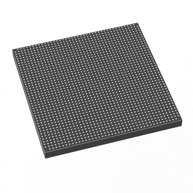
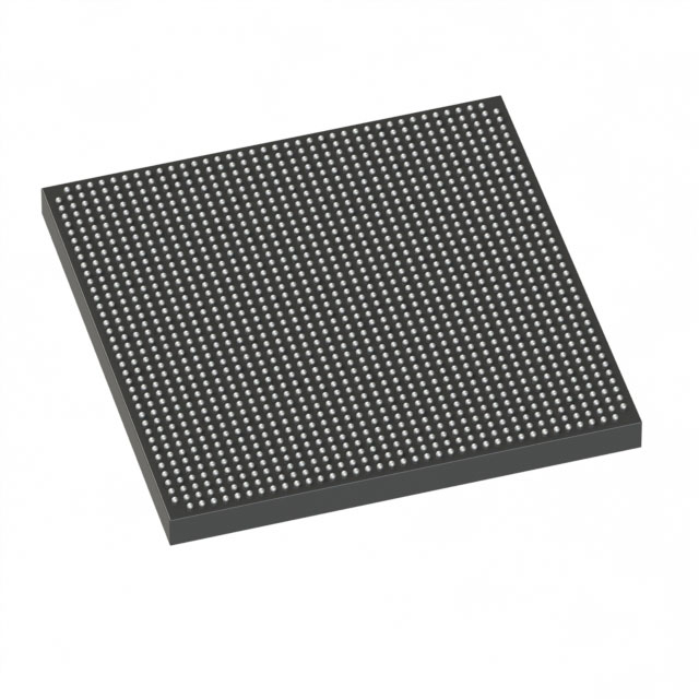
5SGXMB6R1F40C2LG
| Part Description |
Stratix® V GX Field Programmable Gate Array (FPGA) IC 432 53248000 597000 1517-FBGA (40x40) |
|---|---|
| Quantity | 1,576 Available (as of June 15, 2026) |

| Product Category | Field Programmable Gate Array (FPGA) |
|---|---|
| Manufacturer | Intel |
| Manufacturing Status | Active |
| Manufacturer Standard Lead Time | 26 Weeks |
| Datasheet |
Specifications & Environmental
| Device Package | 1517-FBGA (40x40) | Grade | Commercial | Operating Temperature | 0°C – 85°C | ||
|---|---|---|---|---|---|---|---|
| Package / Case | 1517-FBGA (40x40) | Number of I/O | 432 | Voltage | 820 mV - 880 mV | ||
| Mounting Method | Surface Mount | RoHS Compliance | RoHS Compliant | REACH Compliance | REACH Unaffected | ||
| Moisture Sensitivity Level | 3 (168 Hours) | Number of LABs/CLBs | 225400 | Number of Logic Elements/Cells | 597000 | ||
| Number of Gates | N/A | ECCN | N/A | HTS Code | N/A | ||
| Qualification | N/A | Total RAM Bits | 53248000 |
Overview of 5SGXMB6R1F40C2LG – Stratix® V GX Field Programmable Gate Array (FPGA) IC
The 5SGXMB6R1F40C2LG is a Stratix V GX family FPGA in a 1517-FBGA (40x40) surface-mount package. It provides a large programmable logic resource set along with substantial on-chip RAM and a high I/O count, targeted for commercial-grade digital designs.
Key device attributes include approximately 597,000 logic elements, roughly 53.25 Mbits of embedded memory, 432 user I/O pins, a core supply range of 820 mV–880 mV, and an operating temperature range of 0 °C to 85 °C. The device is RoHS compliant.
Key Features
- Core Logic Approximately 597,000 logic elements for large-scale, high-density programmable logic implementations.
- Embedded Memory Approximately 53.25 Mbits of on-chip RAM to support buffering, state storage, and memory-intensive logic functions.
- I/O and Packaging 432 user I/O pins in a 1517-FBGA (40x40) surface-mount package for dense board-level connectivity and compact system integration.
- Power Core supply specified from 820 mV to 880 mV to support the device's internal logic operating window.
- Temperature & Grade Commercial grade operation with an ambient temperature range of 0 °C to 85 °C.
- Standards & Compliance RoHS compliant.
- Family Documentation Device electrical and switching characteristics are covered in the Stratix V device datasheet for detailed design guidance and operating conditions.
Typical Applications
- Complex digital processing Use the large logic element count and embedded RAM to implement wide datapaths, custom accelerators, and algorithmic pipelines.
- High‑density I/O systems 432 I/O pins enable dense interfacing with external peripherals, memory, and high-pin-count connectors.
- Embedded compute and buffering Significant on-chip memory supports buffering, lookup tables, and local storage for streaming or packetized data flows.
- Commercial-grade programmable designs Designed for commercial temperature environments where high logic capacity and integration are required.
Unique Advantages
- Large logic capacity: Approximately 597,000 logic elements reduce the need for multi-device partitioning in complex designs.
- Substantial on-chip memory: About 53.25 Mbits of embedded RAM enables local buffering and memory-intensive functions without external DRAM in many cases.
- High I/O density: 432 I/Os in a compact 1517-FBGA package simplify board routing and support numerous external interfaces.
- Compact surface-mount package: 1517-FBGA (40x40) package provides a balance of pin count and PCB footprint for space-constrained systems.
- Commercial-grade thermal range: Specified operation from 0 °C to 85 °C for standard commercial deployments.
- Regulatory compliance: RoHS compliance for harmonized environmental and manufacturing requirements.
Why Choose 5SGXMB6R1F40C2LG?
This Stratix V GX FPGA offers a combination of high logic capacity, substantial embedded memory, and a large number of I/Os in a compact surface-mount FBGA package, making it well suited for commercial designs that require dense programmable resources and extensive board-level interfacing. The device’s documented electrical and switching characteristics are available through the Stratix V device datasheet to support design validation and integration.
Choose 5SGXMB6R1F40C2LG when your project requires significant on-chip logic and memory resources, a high I/O count, and a commercial temperature-grade FPGA backed by family-level device documentation.
Request a quote or submit a request for pricing and availability to proceed with procurement or design evaluation of 5SGXMB6R1F40C2LG.


Date Founded: 1968
Headquarters: Santa Clara, California, USA
Employees: 130,000+
Revenue: $54.23 Billion
Certifications and Memberships: ISO9001:2015, ISO14001:2015, ISO17025:2017, ISO27001:2022, ISO45001:2018, ISO50001:2018


