
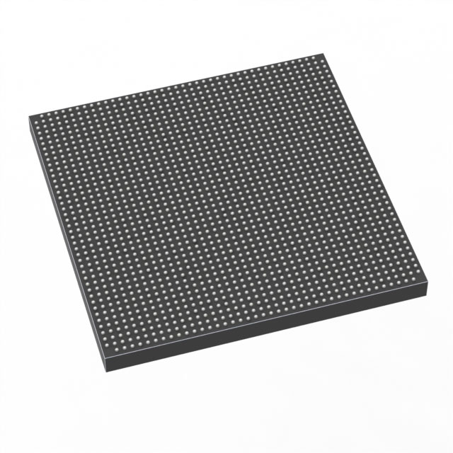
5SGXMB6R1F40C1N
| Part Description |
Stratix® V GX Field Programmable Gate Array (FPGA) IC 432 53248000 597000 1517-FBGA (40x40) |
|---|---|
| Quantity | 93 Available (as of June 15, 2026) |

| Product Category | Field Programmable Gate Array (FPGA) |
|---|---|
| Manufacturer | Intel |
| Manufacturing Status | Obsolete |
| Manufacturer Standard Lead Time | Contact Us |
| Datasheet |
Specifications & Environmental
| Device Package | 1517-FBGA (40x40) | Grade | Commercial | Operating Temperature | 0°C – 85°C | ||
|---|---|---|---|---|---|---|---|
| Package / Case | 1517-FBGA (40x40) | Number of I/O | 432 | Voltage | 870 mV - 930 mV | ||
| Mounting Method | Surface Mount | RoHS Compliance | RoHS Compliant | REACH Compliance | REACH Unknown | ||
| Moisture Sensitivity Level | 3 (168 Hours) | Number of LABs/CLBs | 225400 | Number of Logic Elements/Cells | 597000 | ||
| Number of Gates | N/A | ECCN | 3A001A2C | HTS Code | 8542.39.0001 | ||
| Qualification | N/A | Total RAM Bits | 53248000 |
Overview of 5SGXMB6R1F40C1N – Stratix® V GX Field Programmable Gate Array (FPGA) IC — 597,000 logic elements, 432 I/Os
The 5SGXMB6R1F40C1N is an Intel Stratix® V GX family FPGA supplied in a 1517‑FBGA (40×40) surface‑mount package. It delivers approximately 597,000 logic elements and roughly 53.2 Mbits of embedded RAM, combined with 432 user I/O pins for high‑density digital integration.
Designed as a commercial‑grade device, this FPGA operates from a core supply range of 870 mV to 930 mV and supports an ambient operating temperature range of 0 °C to 85 °C. Its combination of large logic capacity, substantial on‑chip memory, and high I/O count makes it suitable for complex board‑level designs that require dense programmable fabric and on‑chip storage.
Key Features
- High Logic Capacity Approximately 597,000 logic elements provide substantial programmable fabric for complex digital functions and large‑scale integration.
- Embedded Memory Approximately 53.2 Mbits of on‑chip RAM to support buffering, lookup tables, and state storage without relying solely on external memory.
- High I/O Count 432 user I/Os for broad interface support and board‑level connectivity to peripherals, interfaces, and high‑pin‑count systems.
- Package & Mounting Supplied in a 1517‑FBGA (40×40) package, optimized for surface‑mount assembly and compact board placement.
- Power and Core Voltage Core voltage range of 870 mV to 930 mV to match system power domains and enable predictable power planning.
- Commercial Temperature Grade Rated for 0 °C to 85 °C operation, suitable for a broad range of commercial and enterprise applications.
- RoHS Compliant Manufactured to meet RoHS environmental requirements.
Typical Applications
- High‑density digital systems Use the large logic fabric and embedded memory for complex state machines, datapath processing, and custom accelerators on a single device.
- Communications and networking equipment Leverage the high I/O count and on‑chip RAM for board‑level protocol handling, packet buffering, and multi‑lane interfaces.
- Prototyping and system consolidation Integrate multiple functions into a single FPGA to reduce board complexity and accelerate hardware validation.
Unique Advantages
- Large single‑device capacity: The combination of ~597k logic elements and ~53.2 Mbits of RAM enables complex designs without immediate need for multiple FPGAs.
- Extensive I/O flexibility: 432 I/Os provide the pin count required for dense peripheral interfacing and high‑channel designs.
- Compact board footprint: The 1517‑FBGA (40×40) package delivers high integration in a surface‑mount form factor suitable for modern PCB layouts.
- Design predictability: Commercial grade temperature range (0 °C to 85 °C) and defined core voltage range simplify system-level thermal and power planning.
- Regulatory compliance: RoHS compliance supports environmentally constrained product designs.
Why Choose 5SGXMB6R1F40C1N?
The 5SGXMB6R1F40C1N positions itself as a high‑capacity Stratix V GX FPGA for designs that require substantial programmable logic, meaningful on‑chip RAM, and a large number of I/Os in a compact BGA package. It suits teams consolidating multiple board functions into a single device or implementing large stateful and datapath designs that benefit from embedded memory.
Backed by Intel’s Stratix V family lineage, this commercial‑grade FPGA delivers predictable electrical and thermal parameters, enabling designers to plan power, cooling, and signal‑integrity requirements with confidence while leveraging a mature ecosystem for development and support.
Request a quote or submit an inquiry to evaluate 5SGXMB6R1F40C1N for your next high‑density FPGA design.


Date Founded: 1968
Headquarters: Santa Clara, California, USA
Employees: 130,000+
Revenue: $54.23 Billion
Certifications and Memberships: ISO9001:2015, ISO14001:2015, ISO17025:2017, ISO27001:2022, ISO45001:2018, ISO50001:2018


