
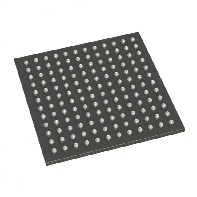
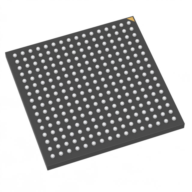
A3P250-1FG144
| Part Description |
ProASIC3 Field Programmable Gate Array (FPGA) IC 97 36864 144-LBGA |
|---|---|
| Quantity | 88 Available (as of June 15, 2026) |
| Product Category | Field Programmable Gate Array (FPGA) |
|---|---|
| Manufacturer | Microchip Technology |
| Manufacturing Status | Active |
| Manufacturer Standard Lead Time | 10 Weeks |
| Datasheet |
Specifications & Environmental
| Device Package | 144-FPBGA (13x13) | Grade | Commercial | Operating Temperature | 0°C – 85°C | ||
|---|---|---|---|---|---|---|---|
| Package / Case | 144-LBGA | Number of I/O | 97 | Voltage | 1.425 V - 1.575 V | ||
| Mounting Method | Surface Mount | RoHS Compliance | RoHS non-compliant | REACH Compliance | REACH Unaffected | ||
| Moisture Sensitivity Level | 3 (168 Hours) | Number of LABs/CLBs | 6144 | Number of Logic Elements/Cells | 6144 | ||
| Number of Gates | 250000 | ECCN | 3A991D | HTS Code | 8542.39.0001 | ||
| Qualification | N/A | Total RAM Bits | 36864 |
Overview of A3P250-1FG144 – ProASIC3 FPGA (144-LBGA)
The A3P250-1FG144 is a ProASIC3 Field Programmable Gate Array (FPGA) from Microchip Technology intended for commercial embedded designs. It provides a mid-range logic capacity with integrated on-chip memory and a dense I/O complement in a compact 144-LBGA package.
With 6,144 logic elements, approximately 36.9 kbits of embedded memory and 97 I/O pins, this device targets applications that require moderate programmable logic, controlled power rails and a small BGA footprint for surface-mount assembly.
Key Features
- Core Logic 6,144 logic elements (cells) and approximately 250,000 gates provide mid-range programmable logic capacity for custom digital functions.
- Embedded Memory Total on-chip RAM of 36,864 bits (approximately 36.9 kbits) to support registers, FIFOs and small buffering requirements.
- I/O Density 97 input/output pins for interfacing with peripherals, sensors and external logic.
- Power Supply Operates from a defined core voltage range of 1.425 V to 1.575 V for predictable power planning.
- Package & Mounting 144-LBGA package (supplier device package: 144-FPBGA, 13×13 mm) designed for surface-mount PCB assembly.
- Operating Range Commercial-grade operating temperature range of 0 °C to 85 °C.
- Compliance RoHS compliant for regulatory alignment in commercial products.
Unique Advantages
- Balanced logic and memory: 6,144 logic elements paired with on-chip RAM support a wide range of mid-size logic implementations without immediate external memory dependence.
- Compact BGA footprint: 144-LBGA (13×13 mm) package enables higher I/O density in space-constrained PCB layouts.
- Predictable power envelope: Narrow core voltage window (1.425 V–1.575 V) simplifies power-supply design and margining.
- Ample I/O count: Ninety-seven I/O pins accommodate multiple peripheral interfaces and signal domains.
- Commercial-grade suitability: Rated for 0 °C to 85 °C operation and RoHS compliant for mainstream commercial product programs.
Why Choose A3P250-1FG144?
The A3P250-1FG144 positions itself as a practical choice for commercial embedded designs that need moderate programmable logic, modest embedded memory and a high I/O count in a compact surface-mount BGA package. Its specifications support integration of custom logic, interfacing and buffering while fitting production workflows that require RoHS compliance and standard commercial temperature ratings.
Manufactured by Microchip Technology and identified as part of the ProASIC3 FPGA family, this device is suited for teams seeking a mid-range FPGA solution that balances integration density, power definition and assembly-friendly packaging.
Request a quote or submit an inquiry to obtain pricing and availability for the A3P250-1FG144.


Date Founded: 1989
Headquarters: Chandler, Arizona, USA
Employees: 22,000+
Revenue: $8.349 Billion
Certifications and Memberships: ISO9001:2015, IATF16949:2016, AS 9100D


