
AFS1500-1FGG256K
| Part Description |
Fusion® Field Programmable Gate Array (FPGA) IC 119 276480 256-LBGA |
|---|---|
| Quantity | 634 Available (as of June 18, 2026) |

| Product Category | Field Programmable Gate Array (FPGA) |
|---|---|
| Manufacturer | Microchip Technology |
| Manufacturing Status | Active |
| Manufacturer Standard Lead Time | 20 Weeks |
| Datasheet |
Specifications & Environmental
| Device Package | 256-FPBGA (17x17) | Grade | Military | Operating Temperature | -55°C – 100°C | ||
|---|---|---|---|---|---|---|---|
| Package / Case | 256-LBGA | Number of I/O | 119 | Voltage | 1.425 V - 1.575 V | ||
| Mounting Method | Surface Mount | RoHS Compliance | ROHS3 Compliant | REACH Compliance | REACH Unaffected | ||
| Moisture Sensitivity Level | 3 (168 Hours) | Number of LABs/CLBs | 38400 | Number of Logic Elements/Cells | 38400 | ||
| Number of Gates | 1500000 | ECCN | 3A991D | HTS Code | 8542.39.0001 | ||
| Qualification | N/A | Total RAM Bits | 276480 |
Overview of AFS1500-1FGG256K – Fusion® Field Programmable Gate Array (FPGA) IC
The AFS1500-1FGG256K is a Fusion® field programmable gate array from Microchip Technology designed for applications requiring moderate logic density and flexible I/O. It integrates 38,400 logic elements and approximately 0.276 Mbits of embedded memory to implement custom digital functions, control logic, and interface glue in space-constrained board designs.
With 119 user I/O, a 256-pin LBGA footprint, and a military-grade operating range, this device targets designs that require reliable operation across wide temperatures and a compact package for surface-mount assembly.
Key Features
- Logic Capacity 38,400 logic elements (cells), enabling implementation of complex custom logic and control functions within a single device.
- Embedded Memory Approximately 0.276 Mbits of on-chip RAM for buffering, small lookup tables, and state storage without external memory.
- I/O Resources 119 user I/O pins to support multiple interfaces, parallel buses, and mixed-signal connectivity on modern PCBs.
- Gate Count 1,500,000 gates providing the fundamental building blocks for combinational and sequential logic designs.
- Power Core voltage supply range of 1.425 V to 1.575 V to match system power rails and ensure predictable power design.
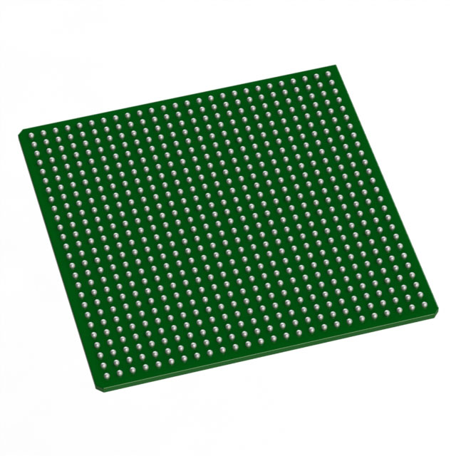
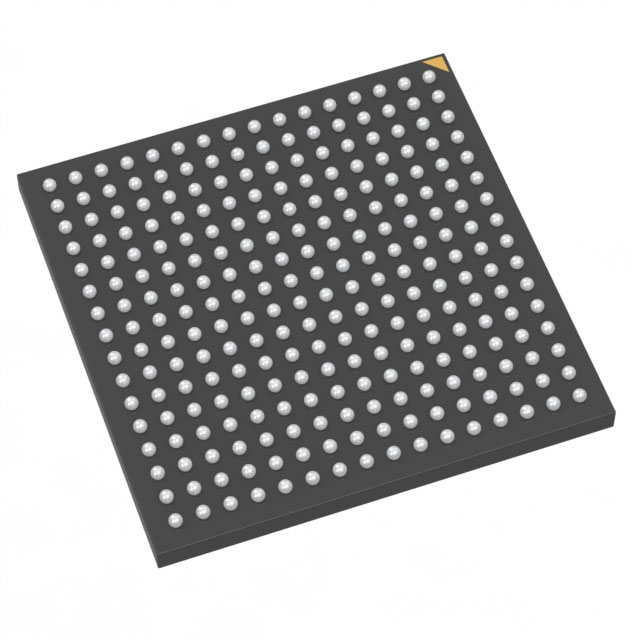
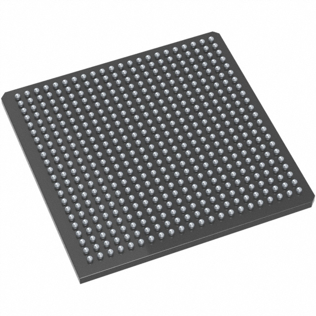
- Package & Mounting 256-LBGA (supplier package 256-FPBGA, 17×17 mm) in a surface-mount form factor for compact board layouts.
- Temperature & Grade Military-grade device with an operating temperature range of −55 °C to 100 °C for demanding environmental use.
- RoHS Compliance RoHS compliant, supporting regulatory requirements for lead-free assembly.
Typical Applications
- Military & Defense Systems Military-grade temperature range and reliability make the device suitable for rugged embedded control, signal routing, and custom processing tasks in defense electronics.
- Embedded Control Compact LBGA package and substantial logic capacity allow integration of control engines, state machines, and interface bridging in constrained PCB real estate.
- High-Density I/O Interfaces 119 I/O pins enable the FPGA to act as a central I/O concentrator for sensor arrays, communication ports, and peripheral expansion.
Unique Advantages
- Substantial Logic Resources: 38,400 logic elements and 1,500,000 gates provide the capacity to consolidate multiple discrete functions into one programmable device, reducing BOM and board complexity.
- On‑Chip Memory: Approximately 0.276 Mbits of embedded RAM supports buffering and local data storage, minimizing or eliminating the need for small external memories.
- Wide Operating Temperature: Rated from −55 °C to 100 °C to support designs that must tolerate extreme thermal conditions without performance compromise.
- Compact Surface-Mount Package: 256-LBGA (256-FPBGA, 17×17) delivers a small footprint for space-constrained systems while maintaining ample I/O connectivity.
- Predictable Power Envelope: Narrow core supply range (1.425 V–1.575 V) simplifies power rail design and voltage margining for reliable operation.
- Regulatory Compliance: RoHS compliant to meet lead-free assembly requirements for commercial and regulated deployments.
Why Choose AFS1500-1FGG256K?
The AFS1500-1FGG256K combines a substantial logic element count, embedded memory, and a broad I/O complement in a compact 256-LBGA package, positioning it for projects that need on-board programmability, moderate density, and dependable operation across extreme temperatures. Its military grade and RoHS compliance make it suitable for long-life and environmentally demanding applications.
Designed and manufactured by Microchip Technology, this Fusion® FPGA delivers a balance of integration, ruggedness, and package efficiency for engineers developing control systems, interface concentrators, and fielded embedded electronics that require configurable logic with defined electrical and environmental specifications.
Request a quote or contact sales to discuss availability, pricing, and to obtain supporting documentation for the AFS1500-1FGG256K.


Date Founded: 1989
Headquarters: Chandler, Arizona, USA
Employees: 22,000+
Revenue: $8.349 Billion
Certifications and Memberships: ISO9001:2015, IATF16949:2016, AS 9100D


