
AGL1000V2-FGG144
| Part Description |
IGLOO Field Programmable Gate Array (FPGA) IC 97 147456 24576 144-LBGA |
|---|---|
| Quantity | 1,733 Available (as of June 18, 2026) |

| Product Category | Field Programmable Gate Array (FPGA) |
|---|---|
| Manufacturer | Microchip Technology |
| Manufacturing Status | Active |
| Manufacturer Standard Lead Time | 8 Weeks |
| Datasheet |
Specifications & Environmental
| Device Package | 144-FPBGA (13x13) | Grade | Commercial | Operating Temperature | 0°C – 70°C | ||
|---|---|---|---|---|---|---|---|
| Package / Case | 144-LBGA | Number of I/O | 97 | Voltage | 1.14 V - 1.575 V | ||
| Mounting Method | Surface Mount | RoHS Compliance | ROHS3 Compliant | REACH Compliance | REACH Unaffected | ||
| Moisture Sensitivity Level | 3 (168 Hours) | Number of LABs/CLBs | 24576 | Number of Logic Elements/Cells | 24576 | ||
| Number of Gates | 1000000 | ECCN | 3A991D | HTS Code | 8542.39.0001 | ||
| Qualification | N/A | Total RAM Bits | 147456 |
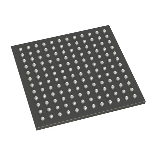
Overview of AGL1000V2-FGG144 – IGLOO FPGA, 24,576 logic elements, 147,456-bit RAM, 97 I/Os, 144-LBGA
The AGL1000V2-FGG144 is a Microchip Technology IGLOO family flash FPGA delivered in a 144-LBGA package. It combines a flash-based, reprogrammable architecture with low-power modes and on-chip embedded memory to address compact, low-power digital designs.
Targeted at commercial embedded and system-integration applications, this device provides substantial logic capacity, dual-port SRAM, and mixed-voltage I/O capability while supporting instant-on behavior and ultra-low standby power modes for power-sensitive designs.
Key Features
- Core Architecture Flash-based IGLOO FPGA architecture fabricated on a flash CMOS process; reprogrammable nonvolatile configuration enables instant-on operation and single-chip solutions.
- Logic Capacity 24,576 logic elements (reported as logic element cells) and approximately 1,000,000 system gates to support complex combinational and sequential logic.
- Embedded Memory 147,456 bits (approximately 144 Kbits) of on-chip true dual-port SRAM for internal data buffering and state storage.
- I/O and Voltage Support 97 user I/Os with family capabilities for bank-selectable, mixed-voltage operation; core supply range specified at 1.14 V to 1.575 V.
- Low-Power Modes Flash*Freeze ultra-low-power retention mode (consumes as little as 5 μW) and Low Power Active operation (static idle from 12 μW) to minimize standby energy while retaining configuration and system state.
- In-System Programming & Security Supports in-system programming with on-chip 128-bit AES decryption and FlashLock® secure configuration to protect FPGA contents (family-level features).
- Packaging & Mounting 144-LBGA package (supplier device package: 144-FPBGA, 13×13 mm) optimized for surface-mount assembly.
- Commercial Temperature Grade Rated for operation from 0 °C to 70 °C and RoHS compliant.
Typical Applications
- Commercial Embedded Systems Compact, reprogrammable logic for control, glue logic, and protocol handling in consumer and commercial devices.
- Battery-Powered & Portable Products Ultra-low standby and active low-power modes enable extended battery life while retaining system state for instant-on responsiveness.
- Single-Chip System Integration / ASIC Replacement High gate and logic element counts with on-chip memory allow consolidation of multiple functions into one FPGA, supporting single-chip solutions.
- Secure Systems & In-System Upgrades On-chip AES decryption and FlashLock® support secure configuration and field updates via JTAG-compliant programming paths.
Unique Advantages
- Low standby and active power: Flash*Freeze retention mode at approximately 5 μW and Low Power Active capability reduce power draw during idle and standby conditions.
- Nonvolatile, reprogrammable configuration: Flash-based configuration retains programmed designs when powered off and enables in-system reprogramming for field updates.
- Substantial logic and memory in a small package: 24,576 logic elements with roughly 147,456 bits of dual-port SRAM and ~1,000,000 system gates in a 144-LBGA footprint.
- Flexible I/O and voltage options: 97 user I/Os combined with family support for bank-selectable, mixed-voltage I/O simplifies interfacing across voltage domains.
- Secure programming features: On-chip 128-bit AES decryption and FlashLock® help protect configuration data and enable secure ISP workflows.
- Commercial-grade reliability and compliance: Surface-mount 144-FPBGA packaging and RoHS compliance align with commercial manufacturing requirements.
Why Choose AGL1000V2-FGG144?
The AGL1000V2-FGG144 positions itself as a compact, low-power FPGA option for commercial embedded designs that require nonvolatile reprogrammability, meaningful logic density, and on-chip dual-port SRAM. Its Flash*Freeze and Low Power Active modes make it suitable for designs where maintaining configuration and minimizing standby energy are priorities.
This part is appropriate for engineering teams looking to consolidate logic, enable field updates, and implement secure, instant-on functionality in a surface-mount 144-LBGA package while staying within commercial temperature limits. The combination of logic capacity, embedded memory, flexible I/O, and on-chip security features supports long-term design scalability and system integration.
Request a quote or submit an RFQ today to obtain pricing and lead-time information for the AGL1000V2-FGG144.


Date Founded: 1989
Headquarters: Chandler, Arizona, USA
Employees: 22,000+
Revenue: $8.349 Billion
Certifications and Memberships: ISO9001:2015, IATF16949:2016, AS 9100D


