
AGLP060V5-CSG289
| Part Description |
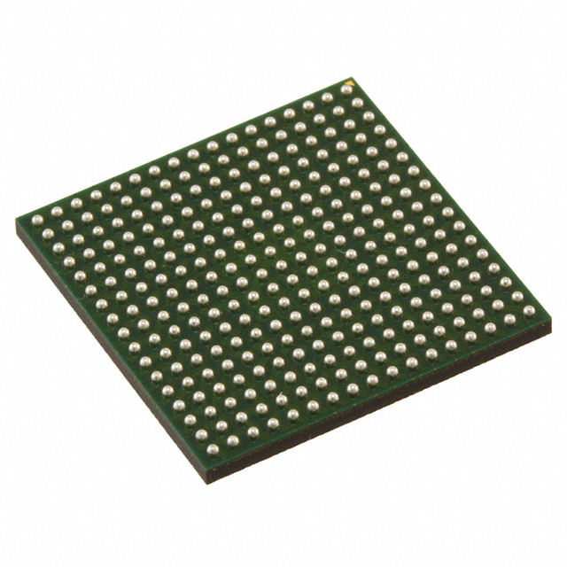
IGLOO PLUS Field Programmable Gate Array (FPGA) IC 157 18432 1584 289-TFBGA, CSBGA |
|---|---|
| Quantity | 329 Available (as of June 15, 2026) |
| Product Category | Field Programmable Gate Array (FPGA) |
|---|---|
| Manufacturer | Microchip Technology |
| Manufacturing Status | Obsolete |
| Manufacturer Standard Lead Time | Contact Us |
| Datasheet |
Specifications & Environmental
| Device Package | 289-CSP (14x14) | Grade | Commercial | Operating Temperature | 0°C – 85°C | ||
|---|---|---|---|---|---|---|---|
| Package / Case | 289-TFBGA, CSBGA | Number of I/O | 157 | Voltage | 1.425 V - 1.575 V | ||
| Mounting Method | Surface Mount | RoHS Compliance | RoHS Compliant | REACH Compliance | REACH Unaffected | ||
| Moisture Sensitivity Level | 3 (168 Hours) | Number of LABs/CLBs | 1584 | Number of Logic Elements/Cells | 1584 | ||
| Number of Gates | 60000 | ECCN | 3A991D | HTS Code | 8542.39.0001 | ||
| Qualification | N/A | Total RAM Bits | 18432 |
Overview of AGLP060V5-CSG289 – IGLOO PLUS Flash FPGA, 1,584 Logic Elements, 289-TFBGA
The AGLP060V5-CSG289 is a Microchip IGLOO PLUS flash-based FPGA in a compact 289-TFBGA package. It delivers a mid-range configurable fabric with 1,584 logic elements, approximately 18,432 bits of embedded RAM and support for nonvolatile on-chip FlashROM—designed for low-power, single-chip system integration in commercial embedded applications.
Built on IGLOO PLUS architecture, this device targets low-power control, interface and glue-logic roles where compact footprint, mixed-voltage I/O and retained configuration are valuable. Key value propositions include nonvolatile flash configuration, ultra-low-power Flash*Freeze capability, and a mix of I/O and clocking resources for flexible system integration.
Key Features
- Logic Capacity — 1,584 logic elements (versatile tiles / flip-flops) delivering approximately 60,000 equivalent system gates for mid-range logic implementations.
- Embedded Memory — 18,432 total RAM bits (≈18 kbits) organized in 4,608-bit blocks; true dual-port SRAM support for efficient data buffering and FIFO implementations.
- Nonvolatile Flash — On-chip reprogrammable FlashROM (1 kbit) for retained design storage and instant-on behavior after power cycles.
- Low-Power Modes — Flash*Freeze ultra-low power retention mode (typical 10 μW for AGLP060 family) plus low-power active capability for static idle operation while remaining functional in the system.
- I/O and Voltage Support — 157 user I/Os with mixed-voltage operation (1.2 V, 1.5 V, 1.8 V, 2.5 V and 3.3 V supported per the IGLOO PLUS family); bank-selectable I/O voltages and selectable input characteristics.
- Clocking and PLL — Integrated Clock Conditioning Circuit blocks with one CCC containing a PLL for clock conditioning, phase shift and multiply/divide capabilities.
- Supply and Package — Core supply specified at 1.425 V to 1.575 V. Surface-mount 289-TFBGA package (supplier device package 289-CSP, 14 × 14) for small-footprint board designs.
- Operating Range and Compliance — Commercial grade operation from 0 °C to 85 °C and RoHS compliant.
Typical Applications
- Battery-powered Embedded Control — Use Flash*Freeze and low-power active modes to implement always-on control functions while minimizing standby energy consumption.
- Consumer and Portable Electronics — Compact 289-TFBGA footprint and mixed-voltage I/Os make the device suitable for user-interface logic, sensor aggregation and protocol bridging.
- Industrial and Instrumentation Interface — Mid-range gate count and true dual-port SRAM enable data buffering, serial/parallel bridging and control glue logic in compact systems.
- Security and In-System Programming — On-chip Flash configuration and family support for secure ISP mechanisms allow protected field updates and retained configurations.
Unique Advantages
- Nonvolatile, Instant-On Configuration: Integrated FlashROM stores the design on-chip so the FPGA retains its configuration without external memory and can resume operation quickly after power-up.
- Ultra-Low Power Retention: Flash*Freeze mode (typical 10 μW for AGLP060) keeps design state, SRAM content and I/O states with minimal energy draw—beneficial for power-sensitive systems.
- Flexible Mixed-Voltage I/O: Bank-selectable I/O voltages and support across common logic levels simplify interfacing to a variety of peripherals and legacy devices.
- Compact, Surface-Mount Package: 289-TFBGA (289-CSP, 14 × 14) enables space-constrained PCB designs while providing 157 user I/Os for connectivity.
- On-Chip Clock Conditioning: Multiple CCC blocks and an integrated PLL provide clock multiplication, phase shift and conditioning without external clocking IP.
- Commercial Grade and RoHS Compliant: Designed for 0 °C to 85 °C operation and compliant with RoHS requirements for broad commercial deployment.
Why Choose AGLP060V5-CSG289?
The AGLP060V5-CSG289 balances mid-range logic capacity with low-power operation and nonvolatile configuration, making it well suited for engineers needing a compact FPGA that retains design state without external configuration memory. Its embedded SRAM, mixed-voltage I/O flexibility, integrated clocking and small 289-TFBGA footprint reduce system BOM and simplify board-level integration.
This part is ideal for designers of commercial embedded systems that require retained configuration, compact form factor, and low standby power. Long-term value is supported by a flash-based architecture for field reprogrammability and immediate-on behavior after power cycles.
Request a quote or submit an inquiry to receive availability and pricing information for the AGLP060V5-CSG289.


Date Founded: 1989
Headquarters: Chandler, Arizona, USA
Employees: 22,000+
Revenue: $8.349 Billion
Certifications and Memberships: ISO9001:2015, IATF16949:2016, AS 9100D


