
AGLP060V5-CSG201
| Part Description |
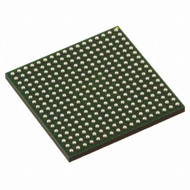
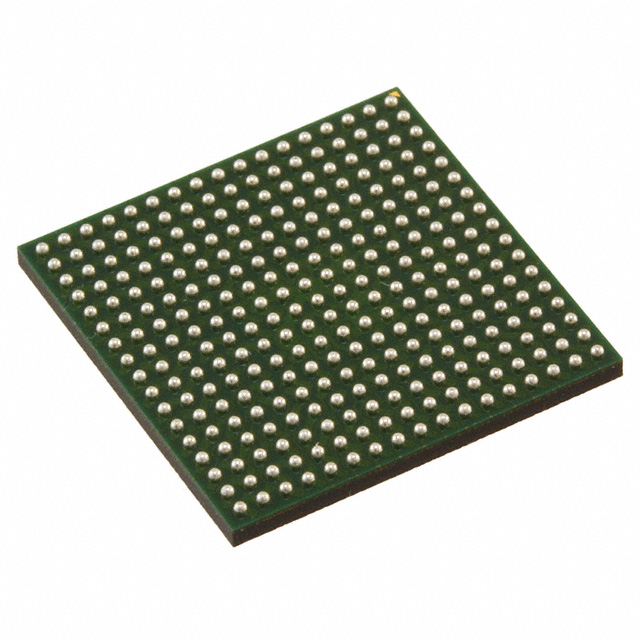
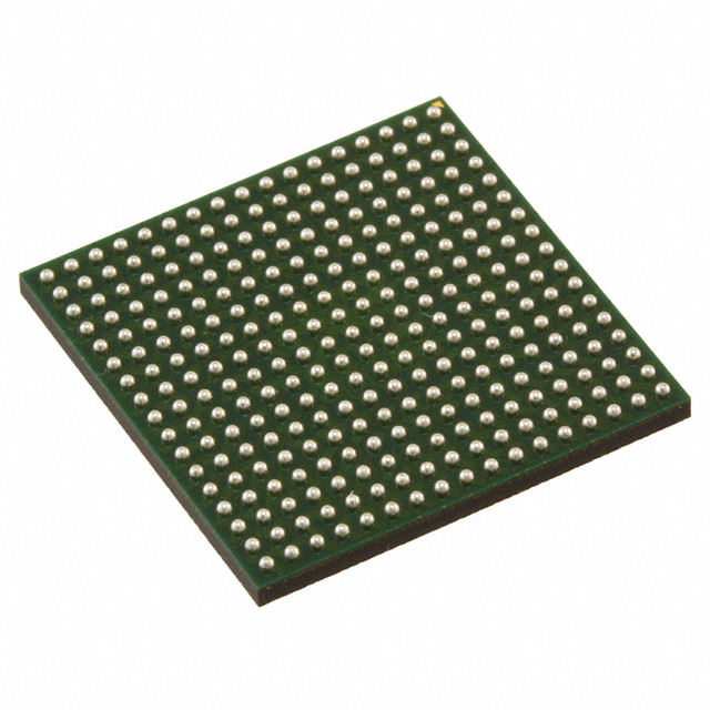
IGLOO PLUS Field Programmable Gate Array (FPGA) IC 157 18432 1584 201-VFBGA, CSBGA |
|---|---|
| Quantity | 517 Available (as of October 8, 2026) |

| Product Category | Field Programmable Gate Array (FPGA) |
|---|---|
| Manufacturer | Microchip Technology |
| Manufacturing Status | Active |
| Manufacturer Standard Lead Time | 8 Weeks |
| Datasheet |
Specifications & Environmental
| Device Package | 201-CSP (8x8) | Grade | Commercial | Operating Temperature | 0°C – 85°C | ||
|---|---|---|---|---|---|---|---|
| Package / Case | 201-VFBGA, CSBGA | Number of I/O | 157 | Voltage | 1.425 V - 1.575 V | ||
| Mounting Method | Surface Mount | RoHS Compliance | ROHS3 Compliant | REACH Compliance | REACH Unaffected | ||
| Moisture Sensitivity Level | 3 (168 Hours) | Number of LABs/CLBs | 1584 | Number of Logic Elements/Cells | 1584 | ||
| Number of Gates | 60000 | ECCN | 3A991D | HTS Code | 8542.39.0001 | ||
| Qualification | N/A | Total RAM Bits | 18432 |
Overview of AGLP060V5-CSG201 – IGLOO PLUS FPGA 201‑VFBGA (CSBGA)
The AGLP060V5-CSG201 is a Microchip IGLOO PLUS flash-based Field Programmable Gate Array (FPGA) in a 201‑VFBGA (CSBGA) package. It combines a 130 nm flash process architecture with low-power operation and on-chip nonvolatile storage to deliver a compact, reprogrammable logic solution for commercial embedded designs.
Targeted at applications requiring low static power, flexible I/O, and moderate logic density, this device provides 60,000 gates, 1,584 logic elements, approximately 18 kbits of embedded RAM, and 157 user I/Os in a small 201‑pin CSP footprint.
Key Features
- Core Logic — 60,000 system gates with 1,584 logic elements (VersaTiles/D‑flip‑flops) suitable for mid-density programmable logic tasks.
- Embedded Memory — Approximately 18.4 kbits (18,432 bits) of on-chip RAM organized for dual-port SRAM use; supports data buffering and local storage.
- Nonvolatile Flash — On-chip reprogrammable FlashROM (1 kbit) retains programmed design and enables instant-on operation and in-system reconfiguration.
- Low-Power Modes — Flash*Freeze and low-power active capabilities described for the IGLOO PLUS family enable ultra-low standby currents and rapid recovery while preserving design state.
- Clocking and PLL — Clock conditioning circuitry with CCC blocks and an integrated PLL provides clock multiplication, division and phase shift capabilities for system timing.
- I/O and Voltage Support — 157 user I/Os with mixed‑voltage operation; I/O banks support multiple voltage domains for flexible interfacing.
- Supply and Temperature — Core supply nominal range 1.425 V to 1.575 V and commercial operating temperature range 0 °C to 85 °C.
- Package — 201‑VFBGA CSBGA package; supplier device package listed as 201‑CSP (8×8) for a compact board footprint.
- Compliance — RoHS compliant for standard commercial deployment.
Typical Applications
- Portable and Battery‑Powered Devices — Low-power modes and instant-on Flash storage make this FPGA suitable for handheld instruments and portable consumer products that require long standby life.
- Embedded Control and Glue Logic — Mid-density logic and abundant I/O enable system control, protocol bridging, and custom peripheral integration in embedded systems.
- Communications and Interface Processing — On-chip RAM and clock conditioning support buffering and timing tasks for moderate-speed serial interfaces and protocol handling.
- User Interfaces and Sensor Aggregation — Reprogrammability and mixed-voltage I/O simplify integration of displays, touch controllers, and multiple sensor domains in commercial equipment.
Unique Advantages
- Low standby power with retained state — Flash*Freeze and low-power active capabilities let the device preserve configuration and I/O states while minimizing power draw.
- Reprogrammable nonvolatile configuration — Built-in FlashROM provides instant-on behavior and field reprogramming without external configuration memory.
- Compact, board‑friendly package — 201‑pin VFBGA/CSBGA (201‑CSP 8×8) reduces PCB area for space-constrained designs.
- Flexible I/O and mixed-voltage support — Multiple I/O banks and voltage options allow direct interfacing to a range of peripherals without extensive level-shifting.
- Integrated clock conditioning — CCC blocks with an integrated PLL provide on-chip timing flexibility to simplify system clock distribution.
Why Choose AGLP060V5-CSG201?
The AGLP060V5-CSG201 offers a balanced combination of mid-range logic capacity, embedded memory, and low-power operation in a compact CSP/FBGA package. Its flash-based nonvolatile configuration and family-level low-power features make it a practical choice for commercial embedded systems that require reprogrammability, retained state across power cycles, and efficient standby behavior.
This device is well suited for designers developing portable electronics, embedded control modules, and interface logic where board space, power consumption, and flexible I/O are key considerations. Its commercial-grade temperature range and RoHS compliance support standard production and assembly processes.
Request a quote or submit an inquiry to receive pricing and availability for the AGLP060V5-CSG201. Our team can provide further technical details and support for your design evaluation.




















Date Founded: 1989
Headquarters: Chandler, Arizona, USA
Employees: 22,000+
Revenue: $8.349 Billion
Certifications and Memberships: ISO9001:2015, IATF16949:2016, AS 9100D




