
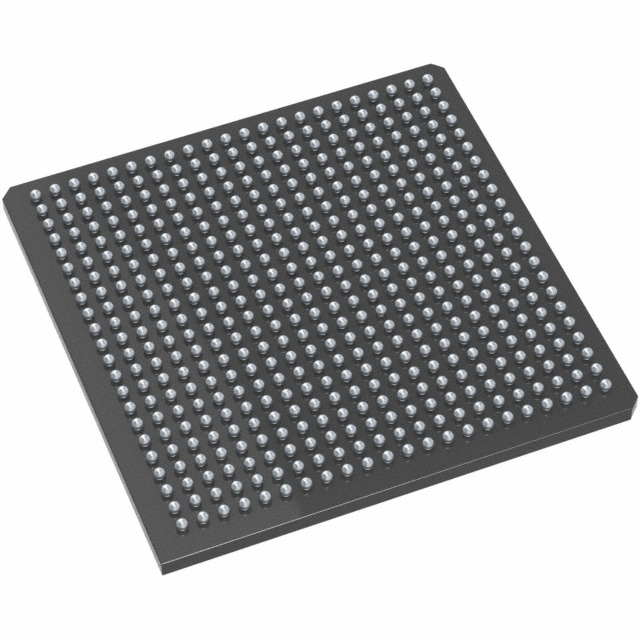
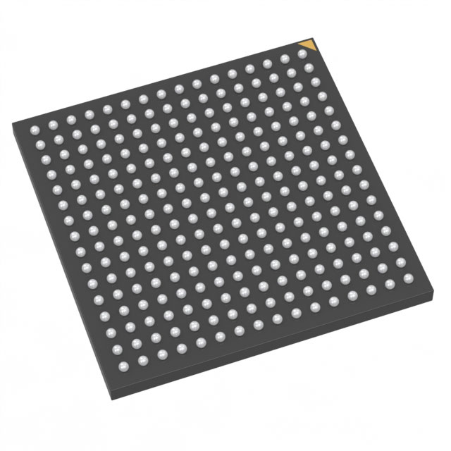
AX250-1FG256I
| Part Description |
Axcelerator Field Programmable Gate Array (FPGA) IC 138 55296 256-LBGA |
|---|---|
| Quantity | 374 Available (as of June 15, 2026) |

| Product Category | Field Programmable Gate Array (FPGA) |
|---|---|
| Manufacturer | Microchip Technology |
| Manufacturing Status | Active |
| Manufacturer Standard Lead Time | 8 Weeks |
| Datasheet |
Specifications & Environmental
| Device Package | 256-FPBGA (17x17) | Grade | Industrial | Operating Temperature | -40°C – 85°C | ||
|---|---|---|---|---|---|---|---|
| Package / Case | 256-LBGA | Number of I/O | 138 | Voltage | 1.425 V - 1.575 V | ||
| Mounting Method | Surface Mount | RoHS Compliance | RoHS non-compliant | REACH Compliance | REACH Unaffected | ||
| Moisture Sensitivity Level | 3 (168 Hours) | Number of LABs/CLBs | 4224 | Number of Logic Elements/Cells | 4224 | ||
| Number of Gates | 250000 | ECCN | 3A991D | HTS Code | 8542.39.0001 | ||
| Qualification | N/A | Total RAM Bits | 55296 |
Overview of AX250-1FG256I – Axcelerator Field Programmable Gate Array (FPGA) IC 138 55296 256-LBGA
The AX250-1FG256I is an Axcelerator antifuse FPGA from Microchip Technology built on the AX architecture. It delivers a nonvolatile, single‑chip FPGA solution with deterministic timing and on‑chip embedded memory and FIFOs, aimed at industrial applications that require secure, high‑performance programmable logic.
This device provides 250,000 equivalent system gates, 4,224 logic elements, approximately 0.055 Mbits (55,296 bits) of embedded RAM, and 138 I/Os in a 256‑ball LBGA package. It supports core supply operation from 1.425 V to 1.575 V and is specified for industrial temperatures (−40 °C to 85 °C).
Key Features
- AX Architecture / Antifuse Technology Single‑chip, nonvolatile antifuse FPGA architecture for one‑time programmable designs and hardware security.
- Logic Density 250,000 equivalent system gates and 4,224 logic elements to implement complex glue logic and processing functions.
- Embedded Memory & FIFOs Approximately 0.055 Mbits (55,296 bits) of embedded RAM with dedicated FIFO control logic for buffering and packet handling.
- I/O and Interface Capability 138 user I/Os with multi‑standard, mixed‑voltage I/O capability across banked structures and support for high‑speed differential interfaces described by the Axcelerator family.
- Performance Family‑level performance characteristics include 350+ MHz system performance and 500+ MHz internal performance; high‑performance embedded FIFOs and LVDS‑capable I/Os.
- Clocking and PLLs Segmentable clock resources and embedded PLLs (family features) with an input range of 14–200 MHz and frequency synthesis capability up to 1 GHz.
- Power and Package Core supply 1.425–1.575 V (nominal 1.5 V), surface‑mount 256‑LBGA (256‑FPBGA 17×17) package suitable for compact board designs.
- Industrial Grade and Compliance Specified for −40 °C to 85 °C operation and RoHS‑compliant.
- Security and Design Protection FuseLock programming technology in the Axcelerator family provides protection against reverse engineering and design theft.
Typical Applications
- High‑speed interface bridging Use the device to implement protocol conversion, lane alignment, and buffering between high‑speed serial or parallel interfaces leveraging embedded FIFOs and LVDS‑capable I/Os.
- Industrial control and instrumentation Implement deterministic control logic, sensor aggregation, and real‑time processing within industrial temperature ranges.
- Packet buffering and data path processing Embedded RAM blocks and FIFO control logic support temporary packet storage, queuing, and data flow management in communication or data acquisition systems.
- Security‑sensitive hardware designs One‑time programmable antifuse technology and FuseLock help protect intellectual property in secure or tamper‑sensitive applications.
Unique Advantages
- Nonvolatile, one‑time programmable solution: Antifuse architecture provides single‑chip, nonvolatile configuration—eliminating the need for external configuration memory.
- Deterministic timing and controllability: AX architecture features allow user‑controllable timing for designs that require predictable behavior.
- Integrated clocking and PLLs: Embedded PLLs and segmentable clocks simplify clock management for multi‑domain and high‑frequency designs.
- Embedded FIFOs and RAM: On‑chip memory and FIFO control reduce external memory dependencies for buffering and packet handling.
- Industrial temperature range: Specified operation from −40 °C to 85 °C for reliability in industrial environments.
- Design protection with FuseLock: Built‑in programming security minimizes risk of reverse engineering or unauthorized design copying.
Why Choose AX250-1FG256I?
The AX250-1FG256I positions itself as a secure, deterministic FPGA option for industrial applications that need a nonvolatile, one‑time programmable device with substantial logic capacity, embedded RAM/FIFOs, and flexible I/O. Its AX antifuse architecture and family‑level performance characteristics make it well suited for designers implementing high‑performance interfaces, buffering, and control logic without relying on external configuration memory.
Engineers and procurement teams seeking an RoHS‑compliant, surface‑mount 256‑LBGA FPGA with industrial temperature capability and built‑in design protection will find the AX250-1FG256I appropriate for medium‑density programmable logic tasks within larger systems.
Request a quote or submit an inquiry to receive pricing and availability information for the AX250-1FG256I.


Date Founded: 1989
Headquarters: Chandler, Arizona, USA
Employees: 22,000+
Revenue: $8.349 Billion
Certifications and Memberships: ISO9001:2015, IATF16949:2016, AS 9100D


