
AX250-1CQ208M
| Part Description |
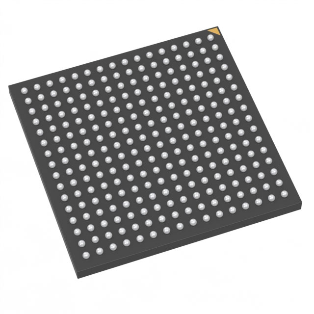
Axcelerator Field Programmable Gate Array (FPGA) IC 115 55296 208-BFCQFP with Tie Bar |
|---|---|
| Quantity | 810 Available (as of June 15, 2026) |

| Product Category | Field Programmable Gate Array (FPGA) |
|---|---|
| Manufacturer | Microchip Technology |
| Manufacturing Status | Active |
| Manufacturer Standard Lead Time | 44 Weeks |
| Datasheet |
Specifications & Environmental
| Device Package | 208-CQFP (75x75) | Grade | Military | Operating Temperature | -55°C – 125°C | ||
|---|---|---|---|---|---|---|---|
| Package / Case | 208-BFCQFP with Tie Bar | Number of I/O | 115 | Voltage | 1.425 V - 1.575 V | ||
| Mounting Method | Surface Mount | RoHS Compliance | RoHS non-compliant | REACH Compliance | REACH Unaffected | ||
| Moisture Sensitivity Level | 3 (168 Hours) | Number of LABs/CLBs | 4224 | Number of Logic Elements/Cells | 4224 | ||
| Number of Gates | 250000 | ECCN | 3A001A2C | HTS Code | 8542.39.0001 | ||
| Qualification | N/A | Total RAM Bits | 55296 |
Overview of AX250-1CQ208M – Axcelerator FPGA IC, 250,000 gates, 115 I/Os, Military Grade
The AX250-1CQ208M is a member of Microchip's Axcelerator antifuse FPGA family implementing the AX architecture. It provides a single-chip, nonvolatile programmable-logic solution with on-chip embedded memory, PLLs, and multi-standard I/O capabilities.
Designed for deployments that demand military-grade temperature range and reliability, the device is suited to systems that require high-performance, deterministic timing and secure in-field programming protection.
Key Features
- AX Antifuse Architecture & Nonvolatile Core Single-chip antifuse FPGA architecture delivering a nonvolatile programmable solution and FuseLock™ programming technology for design protection.
- Logic Capacity Approximately 250,000 equivalent system gates with 4,224 logic elements (cells) to implement complex logic and control functions.
- Embedded Memory & FIFOs Approximately 55 kbits of embedded memory (55,296 bits) with support for embedded FIFO control logic and variable-aspect RAM blocks.
- I/O Resources 115 user I/Os with multi-standard, bank-selectable operation and support for high-speed differential interfaces such as LVDS (700 Mb/s capable).
- Performance Series-level specifications include 350+ MHz system performance and 500+ MHz internal performance, plus embedded FIFOs and PLLs for frequency synthesis.
- Clocking & PLL Embedded phase-locked loop (PLLs) covering a 14–200 MHz input range with frequency synthesis capabilities up to 1 GHz (series-level).
- Package & Mounting Surface-mount 208-BFCQFP with tie bar; supplier device package listed as 208-CQFP (75 × 75 mm footprint).
- Voltage & Temperature Core supply range 1.425 V to 1.575 V and operating temperature range −55 °C to 125 °C (military grade).
- Testability & Security Boundary-scan (IEEE 1149.1 JTAG) support and FuseLock™ programming protection to guard intellectual property.
Typical Applications
- Military and aerospace electronics — Nonvolatile configuration and −55 °C to 125 °C operation for systems requiring extended-temperature, mission-ready logic.
- High-performance communications — Embedded PLLs and LVDS-capable I/Os enable high-speed serial links and protocol bridging.
- Deterministic control and signal processing — Large logic capacity and embedded FIFOs support real-time data-paths and hardware-accelerated processing.
- Secure systems and IP-sensitive designs — FuseLock™ programming technology and antifuse nonvolatile architecture protect design assets.
Unique Advantages
- Nonvolatile single-chip solution: Eliminates external configuration memory and simplifies system design with permanent FPGA configuration.
- Military-grade thermal range: −55 °C to 125 °C operation supports deployment in harsh and mission-critical environments.
- High logic and memory density: 250,000 equivalent gates and ~55 kbits of embedded RAM enable complex, memory-driven designs on a single device.
- Flexible high-speed I/O: Supports mixed-voltage operation and LVDS-capable I/Os for high-bandwidth interfaces and system integration.
- Secure programming and testability: FuseLock™ protection plus IEEE 1149.1 boundary-scan support facilitate secure IP protection and board-level test.
Why Choose AX250-1CQ208M?
The AX250-1CQ208M combines the Axcelerator series' antifuse, nonvolatile architecture with substantial logic capacity, embedded memory, and flexible I/O to deliver a compact, reliable programmable solution for designs that require deterministic performance and extended-temperature operation. Its security and test features help protect intellectual property while easing integration into complex systems.
This device is a fit for engineering teams building high-reliability, high-performance systems that benefit from single-chip nonvolatile FPGA integration, on-chip FIFO/memory resources, and military-grade environmental capability.
Request a quote or submit an inquiry to our sales team for pricing and availability of the AX250-1CQ208M.


Date Founded: 1989
Headquarters: Chandler, Arizona, USA
Employees: 22,000+
Revenue: $8.349 Billion
Certifications and Memberships: ISO9001:2015, IATF16949:2016, AS 9100D


