
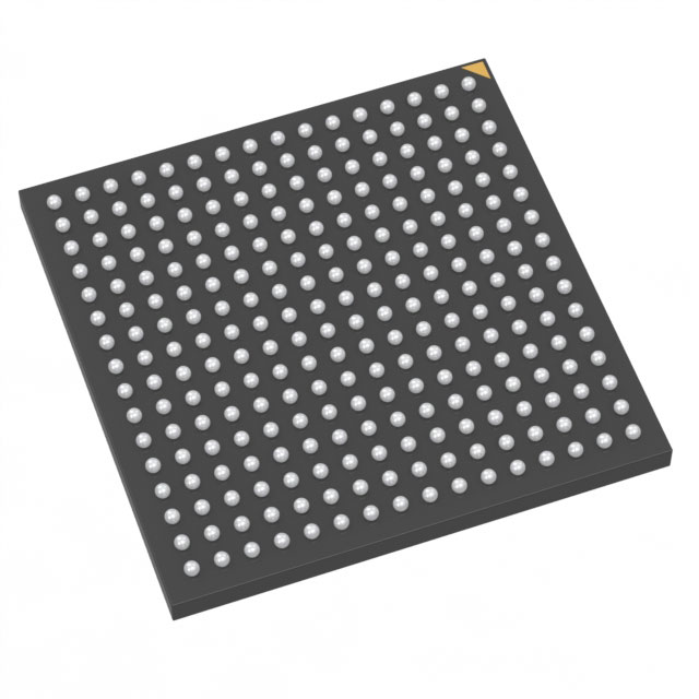
AX250-1FG256M
| Part Description |
Axcelerator Field Programmable Gate Array (FPGA) IC 138 55296 256-LBGA |
|---|---|
| Quantity | 1,470 Available (as of June 15, 2026) |
| Product Category | Field Programmable Gate Array (FPGA) |
|---|---|
| Manufacturer | Microchip Technology |
| Manufacturing Status | Active |
| Manufacturer Standard Lead Time | 16 Weeks |
| Datasheet |
Specifications & Environmental
| Device Package | 256-FPBGA (17x17) | Grade | Military | Operating Temperature | -55°C – 125°C | ||
|---|---|---|---|---|---|---|---|
| Package / Case | 256-LBGA | Number of I/O | 138 | Voltage | 1.425 V - 1.575 V | ||
| Mounting Method | Surface Mount | RoHS Compliance | RoHS non-compliant | REACH Compliance | REACH Unaffected | ||
| Moisture Sensitivity Level | 3 (168 Hours) | Number of LABs/CLBs | 4224 | Number of Logic Elements/Cells | 4224 | ||
| Number of Gates | 250000 | ECCN | 3A001A2C | HTS Code | 8542.39.0001 | ||
| Qualification | N/A | Total RAM Bits | 55296 |
Overview of AX250-1FG256M – Axcelerator Field Programmable Gate Array (FPGA) IC, 250,000 gates, 256-LBGA
The AX250-1FG256M is an Axcelerator antifuse FPGA from Microchip Technology, delivering 250,000 gates in a single-chip, nonvolatile FPGA architecture. Built on a 0.15 μm CMOS antifuse process with seven metal layers, it provides on-chip embedded SRAM with FIFO control logic, segmentable clocks and embedded PLLs for deterministic, high-performance logic implementations.
Targeted for military-grade and other rugged systems, this device combines security-focused programming technology with a wide operating temperature range and surface-mount 256-LBGA packaging to meet demanding deployment environments.
Key Features
- Core Performance — 250,000 gates and 4,224 logic elements deliver substantial combinatorial and registered resources for mid-density FPGA designs.
- Embedded Memory and FIFOs — Approximately 55,296 bits of on-chip RAM organized as configurable RAM blocks; embedded FIFO control logic supports high-performance buffering and data flow control.
- I/O Flexibility — 138 user I/Os with family-level support for mixed-voltage operation (1.5V, 1.8V, 2.5V, 3.3V) and a variety of single-ended and differential standards, enabling flexible interface choices.
- Clocking and PLLs — Segmentable clock resources and embedded PLLs (14–200 MHz input range, frequency synthesis capabilities up to 1 GHz) support precise, deterministic timing and high-speed internal operation.
- Security and Nonvolatile Programming — Antifuse single-chip, nonvolatile architecture with FuseLock programming technology to protect designs from reverse engineering and tampering.
- Robust Operating Range — Military-grade device with operating temperature from -55°C to 125°C and a core voltage supply range of 1.425 V to 1.575 V for deployment in harsh environments.
- Package and Mounting — Surface-mount 256-LBGA package (supplier reference: 256-FPBGA, 17×17) for compact board integration.
- Regulatory — RoHS compliant.
Typical Applications
- Military and Rugged Systems — Military-grade temperature range and antifuse nonvolatile programming make the device suitable for applications that require long-term field reliability and tamper resistance.
- High-Performance Data Pathing — Embedded FIFOs, on-chip SRAM and high internal performance support packet buffering, protocol bridging and data stream management.
- Deterministic Timing Designs — Segmentable clocks and embedded PLLs enable precise timing control for synchronous systems and timing-critical logic.
Unique Advantages
- Single-Chip Nonvolatile Solution: Antifuse architecture eliminates the need for external configuration memory and provides inherent nonvolatility once programmed.
- Design Security: FuseLock programming technology protects against reverse engineering and unauthorized access to bitstream information.
- Wide Temperature Operation: Rated from -55°C to 125°C and specified as military grade, supporting deployment in demanding thermal environments.
- Flexible I/O and Clocking: Bank-selectable, mixed-voltage I/Os and segmentable clock resources with PLLs enable adaptable interfacing and deterministic system timing.
- Compact, Surface-Mount Packaging: 256-LBGA (17×17) package provides a high-density mounting option for space-constrained boards.
- RoHS Compliant: Meets lead-free requirements for modern electronics manufacturing processes.
Why Choose AX250-1FG256M?
The AX250-1FG256M positions itself as a secure, mid-density antifuse FPGA that balances performance, on-chip memory and configurable I/O in a military-grade package. Its single-chip nonvolatile architecture and FuseLock protection are well suited to applications where long-term configurability and design security are priorities.
Designers seeking deterministic timing, embedded FIFO capability and a compact 256-LBGA solution will find the AX250-1FG256M a practical option for rugged and high-reliability systems that require a secure FPGA platform with clear electrical and thermal specifications.
Request a quote or submit a technical inquiry for the AX250-1FG256M to receive pricing and availability information tailored to your project needs.


Date Founded: 1989
Headquarters: Chandler, Arizona, USA
Employees: 22,000+
Revenue: $8.349 Billion
Certifications and Memberships: ISO9001:2015, IATF16949:2016, AS 9100D


