
AX250-1CQ352M
| Part Description |
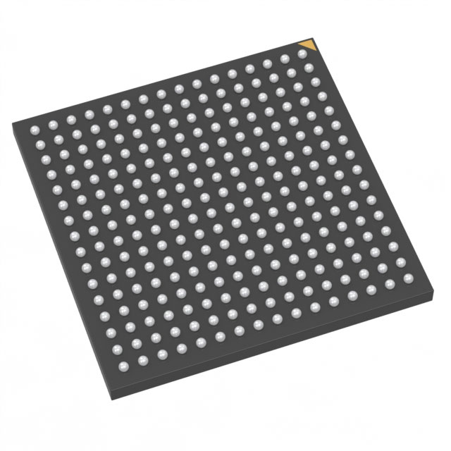
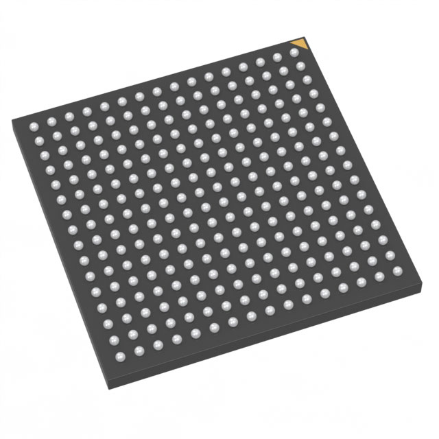
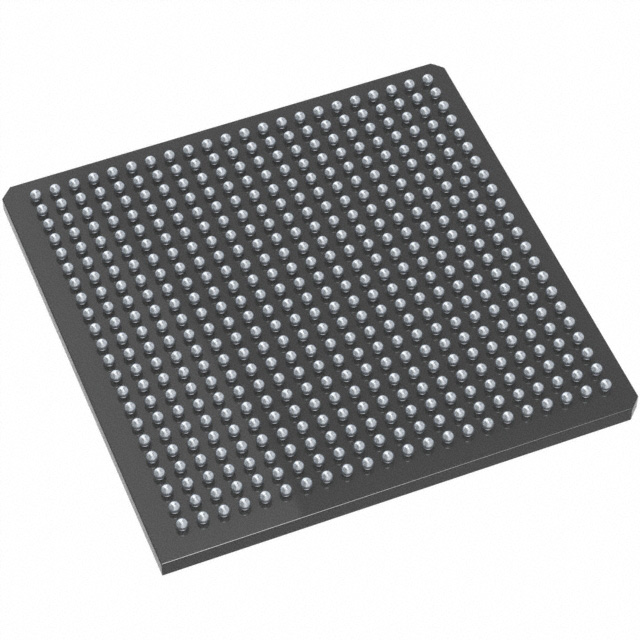
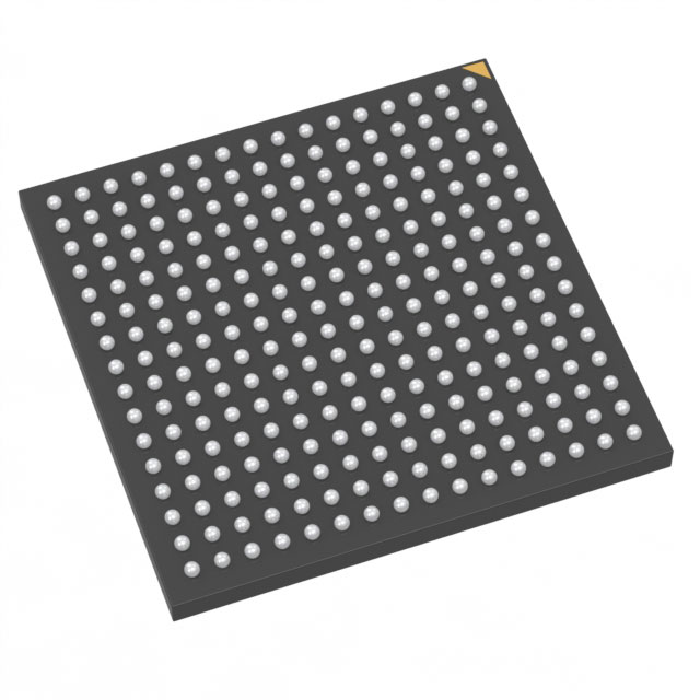
Axcelerator Field Programmable Gate Array (FPGA) IC 198 55296 352-BFCQFP with Tie Bar |
|---|---|
| Quantity | 442 Available (as of October 7, 2026) |

| Product Category | Field Programmable Gate Array (FPGA) |
|---|---|
| Manufacturer | Microchip Technology |
| Manufacturing Status | Active |
| Manufacturer Standard Lead Time | 44 Weeks |
| Datasheet |
Specifications & Environmental
| Device Package | 352-CQFP (75x75) | Grade | Military | Operating Temperature | -55°C – 125°C | ||
|---|---|---|---|---|---|---|---|
| Package / Case | 352-BFCQFP with Tie Bar | Number of I/O | 198 | Voltage | 1.425 V - 1.575 V | ||
| Mounting Method | Surface Mount | RoHS Compliance | RoHS non-compliant | REACH Compliance | REACH Unaffected | ||
| Moisture Sensitivity Level | 3 (168 Hours) | Number of LABs/CLBs | 4224 | Number of Logic Elements/Cells | 4224 | ||
| Number of Gates | 250000 | ECCN | 3A001A2C | HTS Code | 8542.39.0001 | ||
| Qualification | N/A | Total RAM Bits | 55296 |
Overview of AX250-1CQ352M – Axcelerator Field Programmable Gate Array (FPGA), 250,000 gates, 198 I/Os, 352-BFCQFP with Tie Bar
The AX250-1CQ352M is an Axcelerator family antifuse FPGA implementing Microchip's AX architecture. It delivers a nonvolatile, single-chip programmable logic solution with 250,000 equivalent system gates, 4,224 logic elements and embedded SRAM/FIFO resources targeted at high-performance, secure electronic designs.
Built for applications that require high I/O density, deterministic timing and extended temperature operation, the device combines segmentable clocks, on-chip PLLs and embedded FIFO control logic with antifuse-based programming and FuseLock protection to address secure, rugged systems.
Key Features
- Core Logic — 250,000 equivalent system gates and 4,224 logic elements provide substantial combinatorial and sequential resources for complex logic integration.
- Embedded Memory — Approximately 55 kbits of on-chip RAM (55,296 bits) with embedded FIFO control logic and configurable RAM block organizations for flexible data buffering and storage.
- I/O Density & Standards — 198 user I/Os supporting flexible multi-standard, bank-selectable operation and high-speed differential interfaces (series-level LVDS capability up to 700 Mb/s).
- Clocking & PLLs — Segmentable clock resources and on-chip PLLs with a documented input range supporting frequency synthesis to meet demanding timing and high-speed data requirements.
- Nonvolatile Antifuse Technology — Single-chip, nonvolatile antifuse programming technology manufactured on an advanced 0.15 μm CMOS antifuse process with seven metal layers; includes FuseLock protection for design security and reverse-engineering protection.
- Power & Supply — Core voltage supply range: 1.425 V to 1.575 V, supporting low-voltage core operation as specified.
- Package & Mounting — 352-BFCQFP with tie bar (supplier device package: 352-CQFP, 75 × 75 mm) in a surface-mount format for high-pin-count board designs.
- Operating Environment — Military-grade operation rated from −55 °C to 125 °C for use in thermally demanding and rugged environments.
- Compliance — RoHS compliant.
Typical Applications
- Military and Rugged Systems — Military-grade temperature range and antifuse nonvolatile programming make the device suitable for defense electronics and rugged embedded controllers.
- Secure Communications — FuseLock programming and antifuse technology provide a higher level of design security for encryption, secure link processing and classified communications hardware.
- High-Speed Data Interfaces — High I/O count and differential I/O capability support LVDS-enabled serializer/deserializer interfaces and high-throughput data paths.
- Real-Time Signal Processing — Large logic and embedded FIFO resources combined with deterministic timing and PLL synthesis support signal processing tasks requiring predictable latency.
Unique Advantages
- Nonvolatile, One-Time Programmable Architecture: Antifuse-based single-chip programming eliminates the need for external configuration memory and provides permanent programming for secure deployments.
- Design Security with FuseLock: Built-in FuseLock technology protects against reverse engineering and design theft, preserving intellectual property.
- Deterministic Timing Controls: Segmentable clocks and on-chip PLLs enable user-controllable, deterministic timing suited to latency-sensitive designs.
- High I/O Count in a Compact Package: 198 I/Os in a 352-pin CQFP package provide dense connectivity for board-level integration without sacrificing signal options.
- Rugged Temperature Range: Military-grade rating from −55 °C to 125 °C supports operation in harsh thermal environments.
- Embedded Memory and FIFO Support: On-chip RAM blocks with programmable FIFO control simplify buffering and dataflow management inside the FPGA fabric.
Why Choose AX250-1CQ352M?
The AX250-1CQ352M positions itself as a high-performance, secure and rugged FPGA option within the Axcelerator family. With 250,000 equivalent gates, 4,224 logic elements, embedded RAM and a high I/O count in a 352-pin CQFP package, it is well suited to designs that require permanent programming, deterministic timing and elevated design security.
This device is appropriate for engineering teams building defense, secure communications, or other mission-critical systems that demand a nonvolatile FPGA with military-grade temperature capability, on-chip PLLs and extensive I/O and memory resources.
If you would like pricing, availability or to request a quote for the AX250-1CQ352M, submit a quote request or contact sales to receive a tailored response for your project needs.




















Date Founded: 1989
Headquarters: Chandler, Arizona, USA
Employees: 22,000+
Revenue: $8.349 Billion
Certifications and Memberships: ISO9001:2015, IATF16949:2016, AS 9100D




