
AX500-1CQ208M
| Part Description |
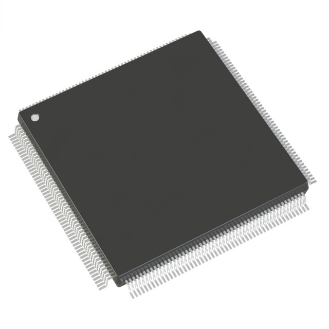
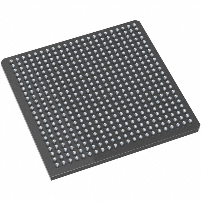
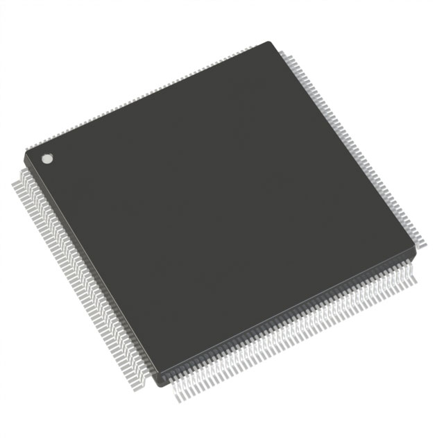
Axcelerator Field Programmable Gate Array (FPGA) IC 115 73728 208-BFCQFP with Tie Bar |
|---|---|
| Quantity | 598 Available (as of October 8, 2026) |

| Product Category | Field Programmable Gate Array (FPGA) |
|---|---|
| Manufacturer | Microchip Technology |
| Manufacturing Status | Active |
| Manufacturer Standard Lead Time | 52 Weeks |
| Datasheet |
Specifications & Environmental
| Device Package | 208-CQFP (75x75) | Grade | Military | Operating Temperature | -55°C – 125°C | ||
|---|---|---|---|---|---|---|---|
| Package / Case | 208-BFCQFP with Tie Bar | Number of I/O | 115 | Voltage | 1.425 V - 1.575 V | ||
| Mounting Method | Surface Mount | RoHS Compliance | RoHS non-compliant | REACH Compliance | REACH Unaffected | ||
| Moisture Sensitivity Level | 3 (168 Hours) | Number of LABs/CLBs | 8064 | Number of Logic Elements/Cells | 8064 | ||
| Number of Gates | 500000 | ECCN | 3A001A2C | HTS Code | 8542.39.0001 | ||
| Qualification | N/A | Total RAM Bits | 73728 |
Overview of AX500-1CQ208M – Axcelerator Field Programmable Gate Array (FPGA) IC, 115 I/Os, 73,728-bit RAM, 208-BFCQFP with Tie Bar
The AX500-1CQ208M is an Axcelerator antifuse FPGA from Microchip Technology built on the AX architecture. This single-chip, nonvolatile FPGA delivers approximately 500,000 equivalent system gates with 8,064 logic elements and on-chip RAM, tailored for applications that require high-performance, secure, and long-term-configurable programmable logic.
Targeted for rugged and mission-critical embedded systems, the device combines high-density logic, flexible multi-standard I/Os and a military-grade operating range to meet demanding deployment environments where reliability and design security matter.
Key Features
- Core Capacity Approximately 500,000 equivalent system gates and 8,064 logic elements for mid-to-high density logic integration.
- Embedded Memory Approximately 0.074 Mbits of on-chip RAM (73,728 bits) to support embedded FIFOs and local data buffering.
- I/O Flexibility 115 user I/Os with Axcelerator family multi-standard support including bank-selectable I/Os and support for single-ended and differential standards as described in the Axcelerator family documentation.
- Clocking and PLLs Segmentable clock resources and embedded PLL capability (family-level specifications include 14–200 MHz input range and frequency synthesis capability) for flexible timing and high-frequency internal operation.
- Performance Family-level performance characteristics include high internal and system switching capability suitable for designs requiring elevated clock rates and throughput.
- Package & Mounting 208-BFCQFP with tie bar (supplier device package: 208-CQFP, 75 × 75) in a surface-mount form factor for board-level assembly.
- Power Core supply specified 1.425 V to 1.575 V, consistent with the 1.5 V family core operation.
- Rugged Operating Range Military-grade device with operating temperature range from −55 °C to 125 °C.
- Design Security & Diagnostics Antifuse, nonvolatile architecture and family-level FuseLock programming technology to protect against reverse engineering, plus in‑system diagnostic and debug capability provided by Microchip tools.
- Environmental Compliance RoHS compliant.
Typical Applications
- Aerospace and Defense Systems Use as mission-critical processing and I/O glue logic where military temperature range, nonvolatile configuration and design security are required.
- High-Speed Communications Deploy for protocol bridging, line cards or custom SERDES-adjacent logic leveraging the family’s high-performance I/O capabilities and embedded FIFOs.
- Secure Embedded Processing Implement application-specific processing and control while protecting intellectual property with the antifuse programming and FuseLock protections.
- Industrial and Ruggedized Equipment Integrate into rugged control and instrumentation platforms that require broad temperature tolerance and long-term field-configurable logic.
Unique Advantages
- Nonvolatile, One-Time Programmable Architecture: Antifuse-based single-chip configuration eliminates the need for external configuration memory and ensures persistent, tamper-resistant operation.
- Design Security (FuseLock): Programming technology specifically intended to protect designs against reverse engineering and unauthorized readout.
- High-Density Logic in a Compact Package: 8,064 logic elements and 500k equivalent gates in a 208-pin CQFP footprint reduce board-level routing and simplify mid-density system designs.
- Rugged Temperature and Military Grade: Specified for −55 °C to 125 °C operation and listed as Military grade for applications with strict environmental requirements.
- On-Chip Memory and FIFO Support: Embedded RAM (73,728 bits) and family-level FIFO control logic reduce external memory dependency for buffering and streaming data paths.
- Vendor Diagnostic Ecosystem: In-system diagnostic and debug capability available through Microchip’s Silicon Explorer tooling for validation and troubleshooting.
Why Choose AX500-1CQ208M?
The AX500-1CQ208M combines a substantial logic footprint with on-chip memory, flexible I/O and military-grade environmental specifications to serve demanding embedded designs that require persistent configuration and strong design protection. Its antifuse, nonvolatile architecture is suited to systems where field reliability and IP security are priorities.
For engineers and procurement teams building rugged communications, defense, or secure embedded platforms, this Axcelerator FPGA offers a balanced mix of density, performance-oriented family features and production-ready packaging that supports long-term deployment and maintainability.
Request a quote or submit an inquiry to get pricing, availability and support information for AX500-1CQ208M.




















Date Founded: 1989
Headquarters: Chandler, Arizona, USA
Employees: 22,000+
Revenue: $8.349 Billion
Certifications and Memberships: ISO9001:2015, IATF16949:2016, AS 9100D




