
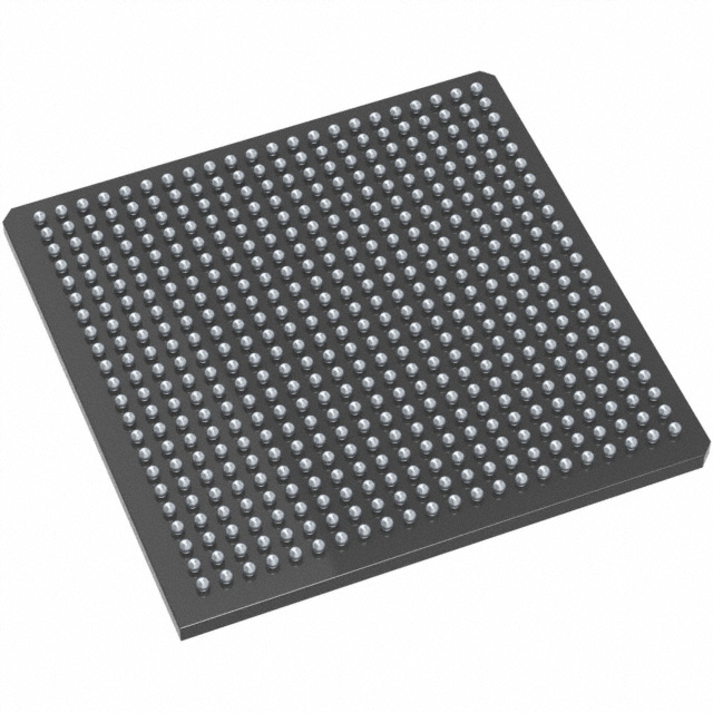
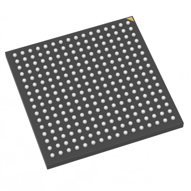
AX250-FGG484M
| Part Description |
Axcelerator Field Programmable Gate Array (FPGA) IC 248 55296 484-BGA |
|---|---|
| Quantity | 153 Available (as of June 15, 2026) |
| Product Category | Field Programmable Gate Array (FPGA) |
|---|---|
| Manufacturer | Microchip Technology |
| Manufacturing Status | Active |
| Manufacturer Standard Lead Time | 16 Weeks |
| Datasheet |
Specifications & Environmental
| Device Package | 484-FPBGA (23x23) | Grade | Military | Operating Temperature | -55°C – 125°C | ||
|---|---|---|---|---|---|---|---|
| Package / Case | 484-BGA | Number of I/O | 248 | Voltage | 1.425 V - 1.575 V | ||
| Mounting Method | Surface Mount | RoHS Compliance | ROHS3 Compliant | REACH Compliance | REACH Unaffected | ||
| Moisture Sensitivity Level | 3 (168 Hours) | Number of LABs/CLBs | 4224 | Number of Logic Elements/Cells | 4224 | ||
| Number of Gates | 250000 | ECCN | 3A001A2C | HTS Code | 8542.39.0001 | ||
| Qualification | N/A | Total RAM Bits | 55296 |
Overview of AX250-FGG484M – Axcelerator FPGA — 248 I/Os, ~55 kbits Embedded RAM, 484‑BGA
The AX250-FGG484M is an Axcelerator field programmable gate array (FPGA) from Microchip Technology built on the AX antifuse architecture. It delivers nonvolatile, single-chip programmable logic with system-level features including segmentable clocks, embedded PLLs and on-chip SRAM/FIFO control logic.
With 250,000 equivalent system gates, 248 user I/Os and military-grade qualification, the AX250-FGG484M addresses designs that require high performance, deterministic timing and secure programming in a compact 484‑BGA footprint.
Key Features
- Core Architecture AX antifuse-based architecture offering a single-chip, nonvolatile solution with up to 250,000 equivalent system gates and deterministic, user-controllable timing.
- Logic Capacity Approximately 4,224 logic elements (modules/registers and combinatorial cells) to implement mid-density logic functions.
- Embedded Memory Approximately 55 kbits of embedded RAM/FIFO (55,296 total bits) with variable-aspect RAM blocks and programmable embedded FIFO control logic.
- I/O Flexibility 248 user I/Os with support for mixed-voltage operation and differential standards including LVDS (700 Mb/s capable); I/O banks and programmable drive/slew control provide interface flexibility.
- Clocking and PLLs Segmentable clock resources plus embedded PLLs supporting a 14–200 MHz input range and frequency synthesis capabilities up to 1 GHz for flexible clock management.
- Performance Datasheet-documented system and internal performance characteristics (350+ MHz system performance and 500+ MHz internal performance) for high-speed designs.
- Security FuseLock™ programming technology to protect against reverse engineering and design theft.
- Power and Supply Core voltage supply range of 1.425 V to 1.575 V for compatible low-voltage system designs.
- Package and Mounting 484‑ball BGA (484‑FPBGA, 23 × 23) surface-mount package for compact board-level integration.
- Environmental Range Military-grade operating temperature from −55 °C to 125 °C.
Typical Applications
- High-speed serial I/O systems Leverage LVDS-capable I/Os and high internal performance for multi-channel, high-throughput interfaces.
- Secure aerospace and defense designs Military-grade temperature range combined with FuseLock programming supports secure, ruggedized applications.
- Embedded memory buffering and FIFOs On-chip RAM and programmable FIFO control simplify data staging and flow control in packet or stream processing.
- Clocking-intensive digital systems Segmentable clocks and integrated PLLs enable complex clock domains and frequency synthesis for synchronized subsystems.
Unique Advantages
- Nonvolatile single-chip solution: Eliminates the need for external configuration memory while providing one-time programmable antifuse reliability.
- Secure programming with FuseLock™: Protects intellectual property by preventing reverse engineering and unauthorized readback.
- Integrated clock and PLL resources: On-chip PLLs and segmentable clocks reduce external clocking complexity and enable precise timing control.
- Mixed-voltage, bank-selectable I/Os: Support for multiple I/O standards and programmable drive strength simplifies multi-domain interfacing.
- Designed for harsh environments: Military-grade temperature rating (−55 °C to 125 °C) supports deployment in demanding applications.
- Compact BGA packaging: 484‑ball FPBGA (23 × 23) package enables dense board-level integration without sacrificing I/O count.
Why Choose AX250-FGG484M?
The AX250-FGG484M combines a secure, nonvolatile antifuse FPGA architecture with mid-range logic capacity, embedded memory, and flexible I/O capabilities to serve applications that require deterministic timing and robust system-level features. Its integrated PLLs, segmentable clocks and programmable I/O make it suitable for designs that demand high internal performance and precise timing control.
This device is well suited for engineers and programs targeting secure, high-performance applications in challenging temperature environments, offering a balance of logic resources, embedded RAM/FIFO capability and a compact 484‑BGA form factor.
Request a quote or submit an inquiry to obtain pricing, availability and lead-time information for the AX250-FGG484M.


Date Founded: 1989
Headquarters: Chandler, Arizona, USA
Employees: 22,000+
Revenue: $8.349 Billion
Certifications and Memberships: ISO9001:2015, IATF16949:2016, AS 9100D


