
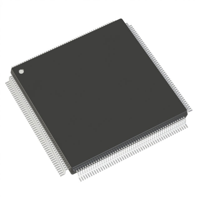
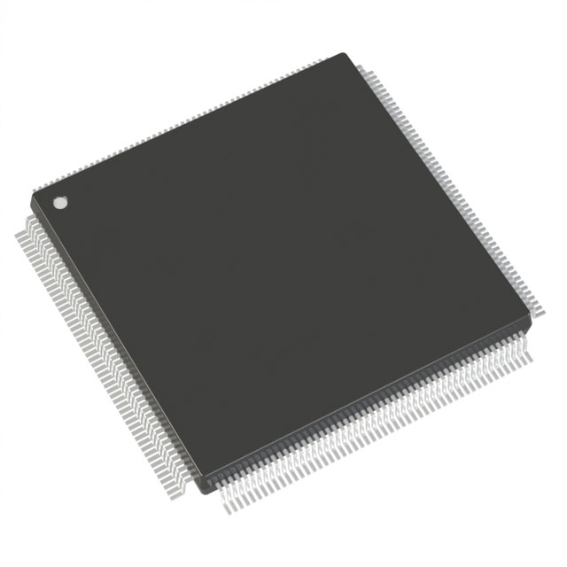
AX250-PQG208M
| Part Description |
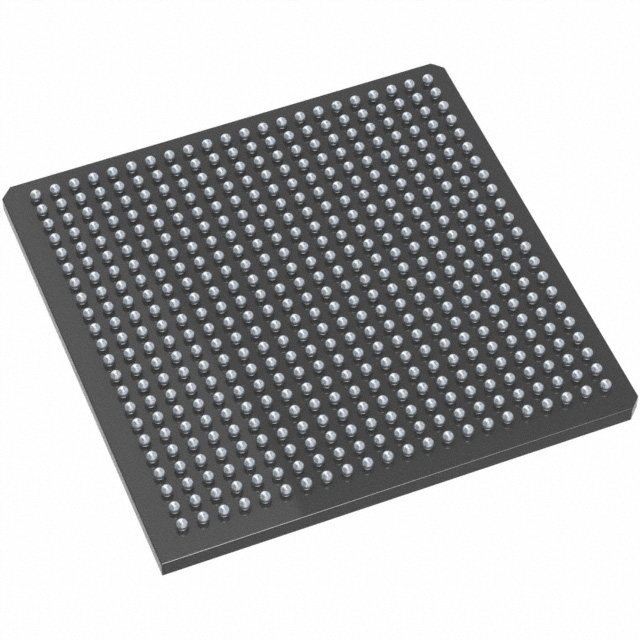
Axcelerator Field Programmable Gate Array (FPGA) IC 115 55296 208-BFQFP |
|---|---|
| Quantity | 376 Available (as of October 7, 2026) |
| Product Category | Field Programmable Gate Array (FPGA) |
|---|---|
| Manufacturer | Microchip Technology |
| Manufacturing Status | Active |
| Manufacturer Standard Lead Time | 16 Weeks |
| Datasheet |
Specifications & Environmental
| Device Package | 208-PQFP (28x28) | Grade | Military | Operating Temperature | -55°C – 125°C | ||
|---|---|---|---|---|---|---|---|
| Package / Case | 208-BFQFP | Number of I/O | 115 | Voltage | 1.425 V - 1.575 V | ||
| Mounting Method | Surface Mount | RoHS Compliance | ROHS3 Compliant | REACH Compliance | REACH Unaffected | ||
| Moisture Sensitivity Level | 3 (168 Hours) | Number of LABs/CLBs | 4224 | Number of Logic Elements/Cells | 4224 | ||
| Number of Gates | 250000 | ECCN | 3A001A2C | HTS Code | 8542.39.0001 | ||
| Qualification | N/A | Total RAM Bits | 55296 |
Overview of AX250-PQG208M – Axcelerator FPGA, 250,000 gates, 208-BFQFP
The AX250-PQG208M is an Axcelerator antifuse Field Programmable Gate Array (FPGA) based on Microchip's AX architecture. It delivers deterministic, single-chip nonvolatile implementation with system-level capabilities including segmentable clocks, embedded FIFOs, and PLL frequency synthesis.
Targeted for military-grade and high-reliability embedded designs, the device provides high internal and system performance coupled with on-chip memory and flexible I/O options to support demanding communications, signal processing, and secure systems operating across a wide temperature range.
Key Features
- Core Performance — Approximately 250,000 equivalent system gates and 4,224 logic elements provide the programmable logic capacity required for mid-density designs.
- Embedded Memory & FIFOs — Approximately 55 kbits (55,296 bits) of embedded SRAM/FIFO with programmable FIFO control logic and variable-aspect RAM blocks for flexible data buffering and storage.
- I/O and Interfaces — 115 user I/Os with support for high-speed differential signaling; datasheet cites LVDS-capable I/Os up to 700 Mb/s and a variety of multi-standard I/O options at mixed voltages.
- Clocking & PLLs — Segmentable clock resources and embedded PLLs with a 14–200 MHz input range and frequency synthesis capabilities up to 1 GHz enable robust timing architectures.
- Nonvolatile Antifuse Technology — Single-chip antifuse programming delivers a nonvolatile configuration and includes FuseLock programming technology for design security and protection against reverse engineering.
- Power — Core supply range of 1.425 V to 1.575 V (nominal 1.5 V) to support low-power core operation.
- Package & Mounting — 208-BFQFP package, surface-mount mounting; supplier device package listed as 208-PQFP (28×28).
- Operating Range & Grade — Military grade with operating temperature range from −55 °C to 125 °C and RoHS-compliant status.
Typical Applications
- Military and Defense Systems — Military-grade temperature range and antifuse nonvolatile configuration suit secure, rugged embedded systems requiring long-term reliability.
- High-Speed Communications — LVDS-capable I/Os and on-chip PLLs support high-throughput serial links and clock synthesis for communications front-ends.
- Embedded Signal Processing — Mid-density logic capacity, dedicated RAM/FIFO blocks, and deterministic timing make the device suitable for buffering, filtering, and protocol processing tasks.
- Secure and IP-Sensitive Designs — Antifuse programming combined with FuseLock technology provides a hardware-based approach to protect intellectual property and prevent reverse engineering.
Unique Advantages
- Single-Chip Nonvolatile Solution: Antifuse architecture eliminates the need for external configuration memory and stores the programmed design on-chip.
- High Deterministic Performance: Documented system and internal performance metrics (350+ MHz system, 500+ MHz internal) and segmentable clocks enable tightly controlled timing for critical paths.
- Integrated Memory and FIFO Support: Embedded SRAM blocks with programmable FIFO logic reduce external memory requirements for many buffering and stream-handling tasks.
- Secure Programming: FuseLock programming technology protects designs from reverse engineering and enhances IP security.
- Wide Thermal and Voltage Operating Range: Military-grade operating temperature (−55 °C to 125 °C) and 1.425–1.575 V core supply support demanding environmental and power conditions.
- Flexible I/O Standards: Bank-selectable and multi-standard I/O support, including high-speed differential signaling, facilitates interoperability across mixed-voltage systems.
Why Choose AX250-PQG208M?
The AX250-PQG208M positions itself as a mid-density, military-grade FPGA that balances performance, on-chip memory, and security. Its antifuse, single-chip nonvolatile architecture combined with embedded FIFOs, PLLs, and flexible I/O options makes it a practical choice for designs that require deterministic behavior, IP protection, and operation across extended temperature ranges.
This device is suited to engineering teams building rugged communications, signal processing, or secure embedded systems that need a reliable, compact FPGA solution with built-in memory and high-speed interface capability.
Request a quote or submit an inquiry to receive pricing, availability, and technical support for AX250-PQG208M.





















Date Founded: 1989
Headquarters: Chandler, Arizona, USA
Employees: 22,000+
Revenue: $8.349 Billion
Certifications and Memberships: ISO9001:2015, IATF16949:2016, AS 9100D




