
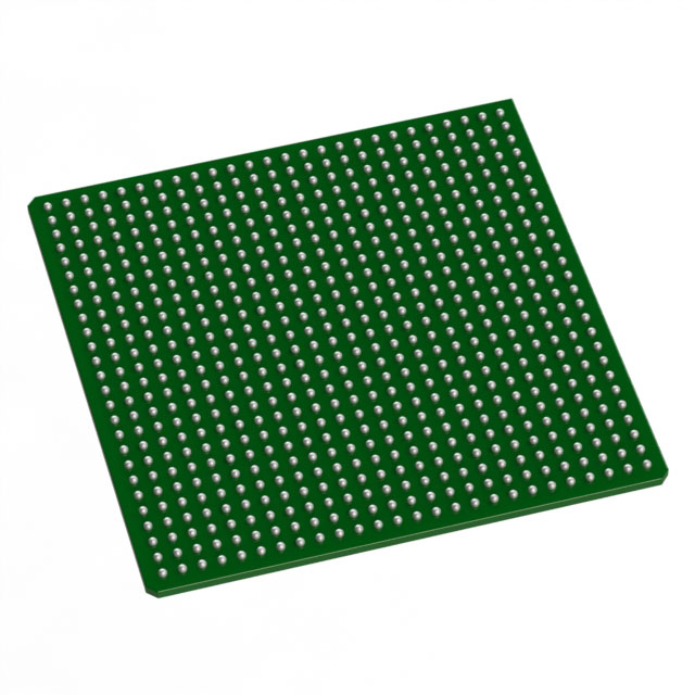
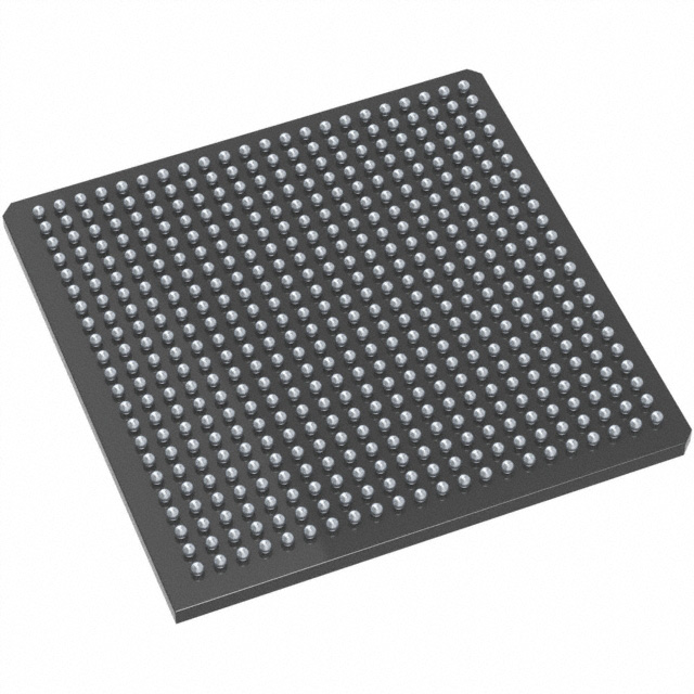
AX500-1FG484M
| Part Description |
Axcelerator Field Programmable Gate Array (FPGA) IC 317 73728 484-BGA |
|---|---|
| Quantity | 992 Available (as of June 10, 2026) |

| Product Category | Field Programmable Gate Array (FPGA) |
|---|---|
| Manufacturer | Microchip Technology |
| Manufacturing Status | Active |
| Manufacturer Standard Lead Time | 16 Weeks |
| Datasheet |
Specifications & Environmental
| Device Package | 484-FPBGA (23x23) | Grade | Military | Operating Temperature | -55°C – 125°C | ||
|---|---|---|---|---|---|---|---|
| Package / Case | 484-BGA | Number of I/O | 317 | Voltage | 1.425 V - 1.575 V | ||
| Mounting Method | Surface Mount | RoHS Compliance | RoHS non-compliant | REACH Compliance | REACH Unaffected | ||
| Moisture Sensitivity Level | 3 (168 Hours) | Number of LABs/CLBs | 8064 | Number of Logic Elements/Cells | 8064 | ||
| Number of Gates | 500000 | ECCN | 3A001A2C | HTS Code | 8542.39.0001 | ||
| Qualification | N/A | Total RAM Bits | 73728 |
Overview of AX500-1FG484M – Axcelerator Field Programmable Gate Array (FPGA) IC 317 73728 484-BGA
The AX500-1FG484M is an Axcelerator antifuse FPGA offering a single-chip, nonvolatile solution based on Microchip's AX architecture and advanced 0.15 µm CMOS antifuse process with seven layers of metal. This device delivers deterministic timing, embedded memory and FIFO control logic, and high-speed I/O capability for applications that require secure, high-performance programmable logic.
Targeted at demanding environments, the AX500-1FG484M provides a balance of logic capacity, on-chip memory and flexible I/O in a 484-ball FPBGA package, with military-grade temperature range and robust programming security features.
Key Features
- Core Capacity and Logic Approximately 500,000 equivalent system gates and 8,064 logic elements provide a substantial resource pool for complex logic and control implementations.
- Embedded Memory and FIFOs Approximately 73,728 bits of embedded SRAM with variable-aspect 4,608-bit RAM blocks and programmable FIFO control logic simplify data buffering and streaming tasks.
- I/O Flexibility 317 user I/Os with multi-standard support including single-ended and differential standards; LVDS-capable I/Os support up to 700 Mb/s for high-speed serial links.
- Clocking and PLL Segmentable clock resources and an embedded PLL (14–200 MHz input range, frequency synthesis up to 1 GHz) enable flexible clock architectures and high-frequency generation.
- Performance Family-level characteristics include 350+ MHz system performance and 500+ MHz internal performance for demanding timing requirements.
- Power and Package 1.425 V to 1.575 V core supply, surface-mount 484-FPBGA (23 × 23) package for compact board integration.
- Reliability and Security Single-chip nonvolatile antifuse technology with FuseLock™ programming protects against reverse engineering; Boundary-scan (JTAG) and unique in-system diagnostic capability with Microchip Silicon Explorer II support manufacturing test and field diagnostics.
- Environmental Range Military-grade operating temperature of −55 °C to +125 °C for use in high-reliability and harsh environments.
- Resource Utilization Architecture supports up to 100% resource utilization with 100% pin locking for predictable, repeatable designs.
Typical Applications
- Military and Aerospace Systems Nonvolatile antifuse configuration, military-grade temperature range and design security make this FPGA suitable for mission-critical avionics, sensors and secure communications equipment.
- High-Speed Data Acquisition and Signal Processing Embedded FIFOs, high internal performance and LVDS-capable I/Os enable efficient buffering and high-throughput data paths for real-time processing.
- Telecommunications and Networking Flexible clocking, high I/O count and PLL frequency synthesis support protocol bridging, packet processing and high-speed interface implementations.
- Test & Measurement Equipment Deterministic timing, boundary-scan support and in-system diagnostics facilitate precision measurement systems and manufacturing test solutions.
Unique Advantages
- Single-Chip Nonvolatile Solution: Eliminates the need for external configuration memory and simplifies system startup and secure deployments.
- High Deterministic Performance: Family performance characteristics (350+ MHz system, 500+ MHz internal) support tight timing margins in advanced designs.
- Flexible, High-Speed I/O: Bank-selectable multi-voltage I/Os and LVDS support up to 700 Mb/s enable diverse interface and signaling options.
- Robust Environmental Capability: Military-grade temperature range (−55 °C to +125 °C) supports use in harsh and temperature-extreme applications.
- Security and IP Protection: FuseLock programming technology and antifuse architecture provide enhanced protection against reverse engineering and design theft.
- Integrated Memory and FIFO Support: On-chip SRAM and programmable FIFO control logic reduce external memory requirements and simplify data-flow designs.
Why Choose AX500-1FG484M?
The AX500-1FG484M positions itself as a secure, high-performance FPGA option for designs that require nonvolatile configuration, deterministic timing and flexible high-speed I/O in a compact BGA package. Its combination of logic resources, embedded memory and PLL-based clocking make it suitable for complex signal-processing, communications and defense-oriented systems.
Developers and procurement teams seeking a rugged, secure programmable-logic solution will find the AX500-1FG484M delivers scalability, on-chip integration and diagnostic capabilities that simplify system design and long-term deployment in challenging environments.
Request a quote or submit an inquiry to get pricing and availability for the AX500-1FG484M.


Date Founded: 1989
Headquarters: Chandler, Arizona, USA
Employees: 22,000+
Revenue: $8.349 Billion
Certifications and Memberships: ISO9001:2015, IATF16949:2016, AS 9100D


