
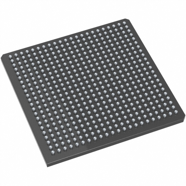
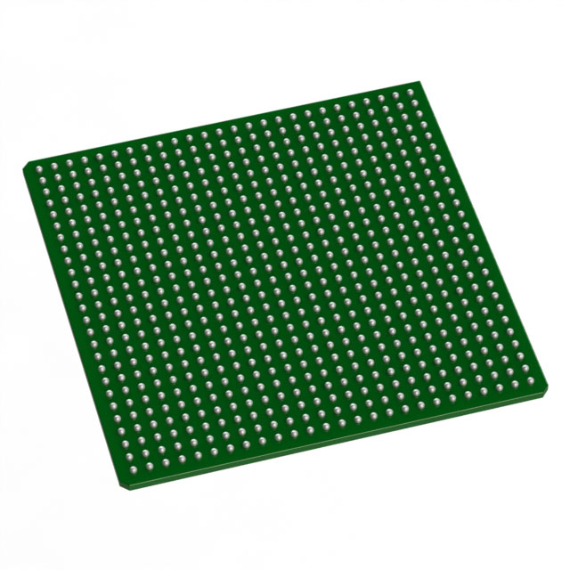
AX500-1FGG484
| Part Description |
Axcelerator Field Programmable Gate Array (FPGA) IC 317 73728 484-BGA |
|---|---|
| Quantity | 1,123 Available (as of June 15, 2026) |

| Product Category | Field Programmable Gate Array (FPGA) |
|---|---|
| Manufacturer | Microchip Technology |
| Manufacturing Status | Active |
| Manufacturer Standard Lead Time | 52 Weeks |
| Datasheet |
Specifications & Environmental
| Device Package | 484-FPBGA (23x23) | Grade | Commercial | Operating Temperature | 0°C – 70°C | ||
|---|---|---|---|---|---|---|---|
| Package / Case | 484-BGA | Number of I/O | 317 | Voltage | 1.425 V - 1.575 V | ||
| Mounting Method | Surface Mount | RoHS Compliance | ROHS3 Compliant | REACH Compliance | REACH Unaffected | ||
| Moisture Sensitivity Level | 3 (168 Hours) | Number of LABs/CLBs | 8064 | Number of Logic Elements/Cells | 8064 | ||
| Number of Gates | 500000 | ECCN | 3A991D | HTS Code | 8542.39.0001 | ||
| Qualification | N/A | Total RAM Bits | 73728 |
Overview of AX500-1FGG484 – Axcelerator FPGA, 500k Gates, 317 I/Os, 484-BGA
The AX500-1FGG484 is an Axcelerator family antifuse FPGA from Microchip Technology, delivering a 500,000-gate-class programmable solution. Built on the AX architecture, the device combines high-performance logic, embedded SRAM/FIFO resources and flexible I/O for demanding embedded designs in commercial applications.
Typical use cases include high-speed data processing, protocol bridging and system control where deterministic timing, integrated memory and robust I/O options accelerate development and reduce system BOM.
Key Features
- Core Capacity — Approximately 500,000 equivalent system gates implemented across 8,064 logic elements, enabling substantial on-chip combinatorial and sequential logic.
- Embedded Memory — Total embedded RAM of 73,728 bits (approximately 0.074 Mbits) suitable for FIFOs and on-chip buffering with family-level embedded FIFO control logic.
- I/O Resources — 317 user I/Os with support in the Axcelerator family for multiple I/O standards and high-speed differential interfaces; family benefits include LVDS-capable channels supporting up to 700 Mb/s.
- Performance — Family-level system performance ratings include 350+ MHz system performance and 500+ MHz internal performance, offering headroom for timing-critical paths.
- Power and Supply — Core voltage supply specified at 1.425 V to 1.575 V for low-voltage operation.
- Package & Mounting — 484-ball BGA package (supplier package: 484-FPBGA, 23×23) designed for surface-mount assembly.
- Commercial Grade & Temperature — Commercial operating temperature range of 0 °C to 70 °C; RoHS compliant.
- System Resources — AX architecture features in-system diagnostic and debug capability and embedded phase-locked loop resources (family-level PLLs with 14–200 MHz input range and frequency synthesis up to 1 GHz).
- Security & Nonvolatile Configuration — Antifuse, single-chip nonvolatile programming with FuseLock programming technology to protect design IP (family-level feature).
Typical Applications
- High-Speed Data Communications — 317 I/Os and Axcelerator family LVDS-capable interfaces support protocol bridging and serial link buffering for telecom and data-path designs.
- Embedded Packet Processing — The combination of 8,064 logic elements and on-chip SRAM/FIFO resources enables packet buffering, framing and custom packet-handling logic.
- Industrial Control & Automation (Commercial) — Deterministic timing, segmentable clock resources and embedded PLLs make the device suitable for control, sequencing and interface aggregation in commercial automation equipment.
- Custom Interface & Protocol Conversion — Flexible, multi-standard I/Os and programmable drive/slew characteristics support mixed-voltage interfaces and bank-selectable I/O configurations for interface adaptation.
Unique Advantages
- Nonvolatile, Antifuse-Based Configuration: Single-chip antifuse programming provides one-time programmable, nonvolatile configuration and inherent protection against configuration loss.
- IP Protection with FuseLock: Family-level FuseLock technology helps protect bitstream and design IP from reverse engineering.
- High Internal Performance: Family-specified internal performance above 500 MHz supports tight timing budgets and high-frequency internal logic.
- Flexible I/O Standards: Bank-selectable, mixed-voltage I/Os and support for multiple single-ended and differential standards enable broad interface compatibility.
- Integrated Timing Resources: Segmentable clocking and embedded PLLs with wide input range and frequency synthesis capability simplify clocking architectures and reduce external components.
- Compact BGA Package: 484-ball FPBGA (23×23) provides a high-pin-count solution in a surface-mount footprint for dense board-level implementations.
Why Choose AX500-1FGG484?
The AX500-1FGG484 positions itself as a high-capacity, commercial-grade FPGA option within the Axcelerator family, offering 500,000 equivalent gates, 8,064 logic elements and embedded RAM to handle complex digital logic, buffering and protocol tasks. Its antifuse nonvolatile architecture and FuseLock protection deliver a secure, single-chip programmed solution for designs where IP protection and deterministic behavior matter.
Designed for engineers needing a high-performance, compact FPGA with flexible I/O and integrated timing/memory resources, this device reduces external component count and supports robust, long-lived commercial deployments backed by Microchip’s Axcelerator family features.
Request a quote or submit an inquiry to evaluate AX500-1FGG484 for your next design and to obtain pricing, availability and ordering information.


Date Founded: 1989
Headquarters: Chandler, Arizona, USA
Employees: 22,000+
Revenue: $8.349 Billion
Certifications and Memberships: ISO9001:2015, IATF16949:2016, AS 9100D


