
AX500-1FGG676
| Part Description |
Axcelerator Field Programmable Gate Array (FPGA) IC 336 73728 676-BGA |
|---|---|
| Quantity | 295 Available (as of June 18, 2026) |
| Product Category | Field Programmable Gate Array (FPGA) |
|---|---|
| Manufacturer | Microchip Technology |
| Manufacturing Status | Active |
| Manufacturer Standard Lead Time | 52 Weeks |
| Datasheet |
Specifications & Environmental
| Device Package | 676-FBGA (27x27) | Grade | Commercial | Operating Temperature | 0°C – 70°C | ||
|---|---|---|---|---|---|---|---|
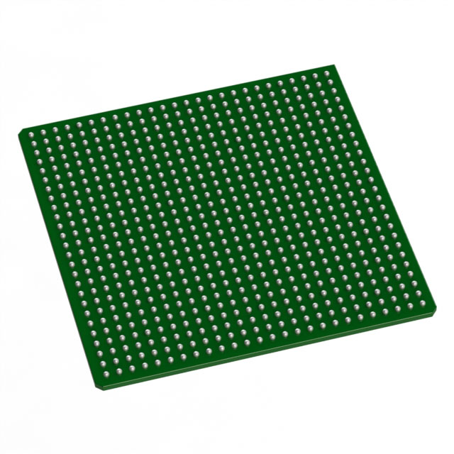
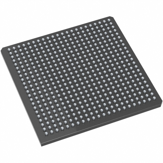
| Package / Case | 676-BGA | Number of I/O | 336 | Voltage | 1.425 V - 1.575 V | ||
| Mounting Method | Surface Mount | RoHS Compliance | ROHS3 Compliant | REACH Compliance | REACH Unaffected | ||
| Moisture Sensitivity Level | 3 (168 Hours) | Number of LABs/CLBs | 8064 | Number of Logic Elements/Cells | 8064 | ||
| Number of Gates | 500000 | ECCN | 3A991D | HTS Code | 8542.39.0001 | ||
| Qualification | N/A | Total RAM Bits | 73728 |
Overview of AX500-1FGG676 – Axcelerator FPGA IC, 336 I/Os, 73,728‑bit RAM, 676‑FBGA
The AX500-1FGG676 is an Axcelerator family Field Programmable Gate Array (FPGA) offered by Microchip Technology. Built on the AX architecture and a CMOS antifuse process, this commercial-grade, nonvolatile FPGA targets applications that require high-performance, deterministic timing and dense I/O integration. Typical use cases include high-speed data interfaces, protocol bridging, embedded memory buffering and custom logic acceleration where predictable timing and compact packaging are important.
Key Features
- Core Capacity — Approximately 500,000 equivalent system gates with 8,064 logic elements, delivering substantial on-chip logic for mid-range FPGA designs.
- Embedded Memory — Approximately 0.074 Mbits (73,728 bits) of embedded RAM/FIFO resources for on-chip buffering and small-data storage requirements.
- I/O Integration — 336 user I/Os with support for multi-standard, bank-selectable signaling; suitable for mixed-voltage I/O systems and high‑density board layouts.
- High-Speed Performance (Series) — Axcelerator family performance characteristics include 350+ MHz system performance and 500+ MHz internal performance, enabling low-latency logic and fast data paths.
- Programmable Clocking — Segmentable clock resources and embedded PLLs support flexible clock architectures and frequency synthesis (series feature set).
- Power and Supply — Core supply range 1.425 V to 1.575 V; designed for low-voltage core operation consistent with the Axcelerator family.
- Package — 676‑ball Fine BGA (676‑FBGA, 27 × 27 mm) surface-mount package optimized for high I/O density and compact board footprint.
- Operating Range — Commercial grade operation from 0 °C to 70 °C, suitable for a wide range of standard electronics environments.
- Security & Reliability (Series) — Nonvolatile antifuse programming and FuseLock™ protection as part of the Axcelerator family for design security and protection against reverse engineering.
- Compliance — RoHS compliant material and manufacturing status.
Typical Applications
- High-Speed Data Interfaces — Use the device’s high internal performance and dense I/O to implement protocol conversion, SERDES-less parallel interfaces, or LVDS-capable links in mid-range systems.
- Embedded FIFO and Buffering — Leverage on-chip SRAM/FIFO resources for data buffering, jitter smoothing, and pipeline staging in streaming or packet-based designs.
- Custom Logic Acceleration — Offload time-critical control and signal-processing tasks from host processors by implementing deterministic hardware logic and tight timing control.
- Mixed‑Voltage System Glue Logic — Bank-selectable, multi-standard I/Os enable interfacing between 1.5 V, 1.8 V, 2.5 V and 3.3 V domains in complex boards.
Unique Advantages
- Deterministic Timing: Segmentable clocks and embedded PLLs provide predictable, user-controllable timing for latency‑sensitive designs.
- Nonvolatile Single‑Chip Solution: Antifuse-based, one-time-programmable architecture eliminates the need for external configuration memory.
- High I/O Density in a Compact Package: 336 I/Os in a 676‑FBGA footprint reduces board routing complexity while supporting dense connector and peripheral integration.
- Integrated Memory for Buffers: Built-in SRAM/FIFO memory simplifies designs that require on-chip buffering without adding external RAM devices.
- Security Features: FuseLock™ programming technology helps protect intellectual property and design integrity.
- RoHS Compliant: Supports regulatory and environmental requirements for many commercial electronic products.
Why Choose AX500-1FGG676?
The AX500-1FGG676 combines a strong mid-range logic capacity with dense I/O and embedded memory to address applications that require compact, deterministic hardware acceleration and interface consolidation. Its antifuse, single-chip nonvolatile architecture simplifies system boot/configuration and enhances design security.
This part is well suited to designers and procurement teams building commercial-grade products that demand predictable timing, mixed-voltage I/O flexibility, and integrated buffering without relying on external configuration devices. The Axcelerator family support features such as high internal performance, PLL-based clock synthesis and robust I/O options provide long-term design scalability within the family.
Request a quote or submit a product inquiry to receive pricing, availability and ordering information for AX500-1FGG676. Our team can provide additional technical details and support for integration into your design.


Date Founded: 1989
Headquarters: Chandler, Arizona, USA
Employees: 22,000+
Revenue: $8.349 Billion
Certifications and Memberships: ISO9001:2015, IATF16949:2016, AS 9100D


