
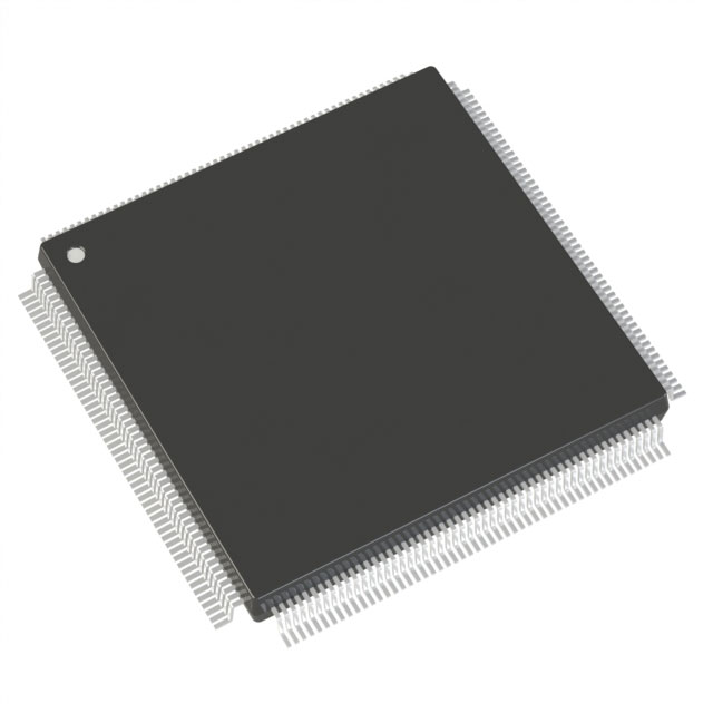
AX500-1PQG208M
| Part Description |
Axcelerator Field Programmable Gate Array (FPGA) IC 115 73728 208-BFQFP |
|---|---|
| Quantity | 980 Available (as of June 15, 2026) |
| Product Category | Field Programmable Gate Array (FPGA) |
|---|---|
| Manufacturer | Microchip Technology |
| Manufacturing Status | Active |
| Manufacturer Standard Lead Time | 16 Weeks |
| Datasheet |
Specifications & Environmental
| Device Package | 208-PQFP (28x28) | Grade | Military | Operating Temperature | -55°C – 125°C | ||
|---|---|---|---|---|---|---|---|
| Package / Case | 208-BFQFP | Number of I/O | 115 | Voltage | 1.425 V - 1.575 V | ||
| Mounting Method | Surface Mount | RoHS Compliance | ROHS3 Compliant | REACH Compliance | REACH Unaffected | ||
| Moisture Sensitivity Level | 3 (168 Hours) | Number of LABs/CLBs | 8064 | Number of Logic Elements/Cells | 8064 | ||
| Number of Gates | 500000 | ECCN | 3A001A2C | HTS Code | 8542.39.0001 | ||
| Qualification | N/A | Total RAM Bits | 73728 |
Overview of AX500-1PQG208M – Axcelerator FPGA, 500,000 gates, 115 I/Os, 208-BFQFP
The AX500-1PQG208M is an Axcelerator antifuse Field Programmable Gate Array (FPGA) from Microchip Technology based on the AX architecture. This single-chip, nonvolatile FPGA integrates segmentable clocks, PLLs, embedded SRAM with FIFO control logic, and high-density routing to deliver deterministic timing and secure designs.
Targeted for applications requiring high performance and design security, the device provides a combination of on-chip memory, logic capacity and flexible I/O in a 208-BFQFP surface-mount package rated for military temperature ranges.
Key Features
- Core Capacity — 500,000 equivalent system gates with 8,064 logic elements to implement complex logic and control functions.
- Embedded Memory & FIFOs — Total on-chip RAM of 73,728 bits (approximately 0.074 Mbits) with embedded FIFO control logic for buffering and data flow management.
- High-Speed Performance — Family-level performance characteristics include 350+ MHz system performance and 500+ MHz internal performance for demanding timing requirements.
- Flexible I/O — 115 user I/Os with LVDS-capable interfaces rated to 700 Mb/s and multi‑standard, mixed-voltage I/O support as provided by the Axcelerator family architecture.
- Clocking and PLLs — Segmentable clock resources plus embedded PLLs; PLL input range 14–200 MHz with frequency synthesis capabilities up to 1 GHz.
- Security & Programmability — Antifuse, single-chip, nonvolatile architecture with FuseLock programming technology to protect against reverse engineering and design theft.
- Package & Mounting — Surface-mount 208-BFQFP (supplier device package listed as 208-PQFP, 28 × 28) for board-level deployment.
- Power and Temperature — Core supply voltage range 1.425 V to 1.575 V; rated operating temperature −55 °C to 125 °C for military-grade environments.
- Standards & Testability — Boundary-scan testing compliant with IEEE 1149.1 (JTAG) and in-system diagnostic/debug capability as described in product documentation.
- Compliance — RoHS compliant.
Typical Applications
- Secure, nonvolatile logic consolidation — Use the antifuse-based Axcelerator FPGA for designs that require one-time programmable, nonvolatile implementation with built-in anti-tamper programming technology.
- High-speed serial interfaces — Leverage LVDS-capable I/Os and embedded FIFOs for buffering and transporting high-rate serial data.
- Timing- and clock-sensitive systems — Employ segmentable clocks and embedded PLLs for deterministic timing, clock distribution and frequency synthesis.
- Defense and military electronics — Suitable for systems requiring military temperature range operation (−55 °C to 125 °C) and ruggedized deployment.
Unique Advantages
- Single-chip, nonvolatile solution: Antifuse architecture provides a nonvolatile programmed configuration that eliminates the need for external configuration memory.
- Design security with FuseLock: Programming technology protects against reverse engineering and design theft, supporting secure IP implementations.
- Deterministic timing and on-chip PLLs: Segmentable clock networks and on-chip PLLs enable controlled, repeatable timing necessary for real-time and synchronous systems.
- High-performance I/O and embedded FIFOs: LVDS-capable I/Os and embedded FIFO control logic facilitate high-throughput data movement and interface flexibility.
- Military temperature range: Rated from −55 °C to 125 °C to meet demanding environmental requirements without external conditioning.
- Comprehensive test and debug support: Boundary-scan (IEEE 1149.1) and in-system diagnostic/debug features simplify validation and bring-up.
Why Choose AX500-1PQG208M?
The AX500-1PQG208M positions itself as a high-performance, secure, nonvolatile FPGA option for designs that demand deterministic timing, robust I/O performance and military-grade temperature operation. Its combination of 500,000 gates, 8,064 logic elements, embedded SRAM/FIFO resources and PLL-based clocking delivers a compact, integrated solution for advanced system designs.
Backed by Axcelerator family features and Microchip Technology programming capabilities, this device is suitable for customers seeking a secure, high-throughput FPGA platform with on-chip memory and flexible I/O in a 208-BFQFP surface-mount package.
Request a quote or submit an inquiry to get pricing and availability for the AX500-1PQG208M. Our team can provide additional technical documentation and ordering information upon request.


Date Founded: 1989
Headquarters: Chandler, Arizona, USA
Employees: 22,000+
Revenue: $8.349 Billion
Certifications and Memberships: ISO9001:2015, IATF16949:2016, AS 9100D


