
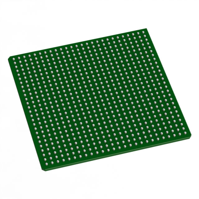
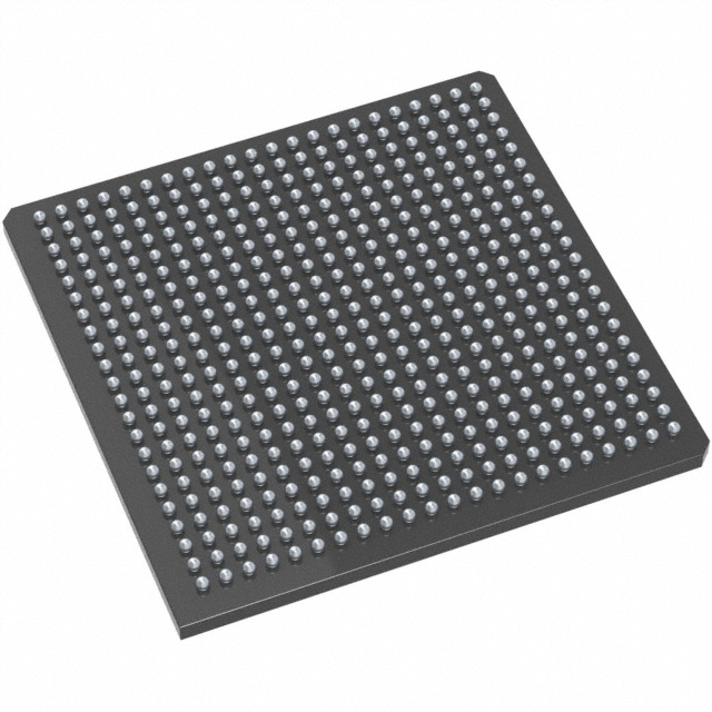
AX500-2FG484I
| Part Description |
Axcelerator Field Programmable Gate Array (FPGA) IC 317 73728 484-BGA |
|---|---|
| Quantity | 524 Available (as of June 18, 2026) |

| Product Category | Field Programmable Gate Array (FPGA) |
|---|---|
| Manufacturer | Microchip Technology |
| Manufacturing Status | Active |
| Manufacturer Standard Lead Time | 8 Weeks |
| Datasheet |
Specifications & Environmental
| Device Package | 484-FPBGA (23x23) | Grade | Industrial | Operating Temperature | -40°C – 85°C | ||
|---|---|---|---|---|---|---|---|
| Package / Case | 484-BGA | Number of I/O | 317 | Voltage | 1.425 V - 1.575 V | ||
| Mounting Method | Surface Mount | RoHS Compliance | RoHS non-compliant | REACH Compliance | REACH Unaffected | ||
| Moisture Sensitivity Level | 3 (168 Hours) | Number of LABs/CLBs | 8064 | Number of Logic Elements/Cells | 8064 | ||
| Number of Gates | 500000 | ECCN | 3A991D | HTS Code | 8542.39.0001 | ||
| Qualification | N/A | Total RAM Bits | 73728 |
Overview of AX500-2FG484I – Field Programmable Gate Array, 317 I/Os, 484-BGA
The AX500-2FG484I Axcelerator Field Programmable Gate Array (FPGA) from Microchip Technology is a single-chip, nonvolatile antifuse FPGA built on the AX architecture. It delivers up to 500,000 equivalent system gates with 8,064 logic elements and approximately 73,728 bits of embedded RAM, targeting high-performance, deterministic embedded logic implementations.
Designed for industrial use, the device offers 317 user I/Os in a 484-ball fine-pitch BGA (23 × 23) package, a 1.425–1.575 V core supply range and an operating temperature range of −40 °C to 85 °C—making it suitable for demanding embedded and communications applications that require reliable, long-term configuration.
Key Features
- Core & Architecture Antifuse-based Axcelerator (AX) architecture providing a single-chip, nonvolatile solution with FuseLock programming technology to protect designs from reverse engineering.
- Logic Capacity Approximately 500,000 equivalent system gates implemented as 8,064 logic elements to support complex custom logic and control functions.
- Embedded Memory & FIFOs Approximately 73,728 bits of embedded RAM with variable-aspect RAM blocks and programmable embedded FIFO control logic for buffering and data management.
- I/O Flexibility 317 user I/Os with multi-standard, bank-selectable operation; LVDS-capable channels supporting high-speed differential signaling up to 700 Mb/s as stated in the device family documentation.
- Performance & Timing System-level performance characteristics cited for the Axcelerator family include 350+ MHz system performance and 500+ MHz internal performance, with segmentable clock resources and embedded PLLs providing frequency synthesis up to 1 GHz.
- Power & Voltage Low-voltage core operation with a specified supply range of 1.425 V to 1.575 V to support power-sensitive designs.
- Package & Mounting 484-ball fine-pitch BGA (484-FPBGA, 23 × 23) surface-mount package for compact board-level integration.
- Industrial Grade & Temperature Industrial-grade device with an operating range of −40 °C to 85 °C for deployment in industrial environments.
- Diagnostics & Test In-system diagnostic and debug capability with Microchip Silicon Explorer II and boundary-scan testing compliant with IEEE 1149.1 (JTAG) as detailed in the product family documentation.
- Compliance RoHS-compliant manufacturing and lead-free packaging options consistent with industry environmental requirements.
Typical Applications
- High-Speed Data Interfacing Use the device’s LVDS-capable I/Os and high-performance internal timing for high-speed serial and parallel data interfaces requiring deterministic timing.
- Embedded Packet Buffering and FIFO Control Leverage the programmable embedded FIFO control logic and on-chip RAM blocks for data buffering in communication and streaming applications.
- Industrial Control and Automation Industrial-grade temperature range and robust single-chip nonvolatile configuration make the FPGA suitable for control logic, motor control sequencing, and machine interface tasks.
- Custom Protocol and Interface Bridging Reconfigure logic elements to implement protocol conversion or custom interface functions while using the device’s PLLs and clock segmentation for accurate timing.
Unique Advantages
- Single-Chip, Nonvolatile Configuration: Antifuse-based, one-time programmable architecture provides permanent configuration without external configuration memory.
- Deterministic Timing and High Internal Speed: Family-documented internal performance and segmentable clocks enable predictable timing closure for latency-sensitive logic.
- Flexible, Multi-Standard I/Os: Bank-selectable I/O voltages and support for both single-ended and differential standards allow interface flexibility across mixed-voltage systems.
- Embedded FIFO and Memory Control: On-chip RAM blocks with programmable FIFO logic simplify buffering and reduce external memory requirements.
- Industrial Temperature Range: −40 °C to 85 °C rating supports deployment in a wide range of industrial environments.
- Design Protection: FuseLock programming technology provides protection against reverse engineering and design theft as described for the device family.
Why Choose AX500-2FG484I?
The AX500-2FG484I combines a substantial logic capacity—approximately 500,000 equivalent system gates and 8,064 logic elements—with embedded memory and FIFO control to address complex, high-throughput embedded designs. Its antifuse, single-chip, nonvolatile configuration model reduces system-level BOM and delivers stable, tamper-resistant implementations.
With industrial temperature capability, a compact 484-FPBGA package, deterministic timing resources including PLLs and segmentable clocks, and flexible I/O standards, this Axcelerator FPGA is positioned for engineers and procurement teams designing robust communication, control, and interface-centric systems that require reliable long-term configuration and high internal performance.
Request a quote or submit a pricing inquiry to receive availability and purchasing information for AX500-2FG484I.


Date Founded: 1989
Headquarters: Chandler, Arizona, USA
Employees: 22,000+
Revenue: $8.349 Billion
Certifications and Memberships: ISO9001:2015, IATF16949:2016, AS 9100D


