
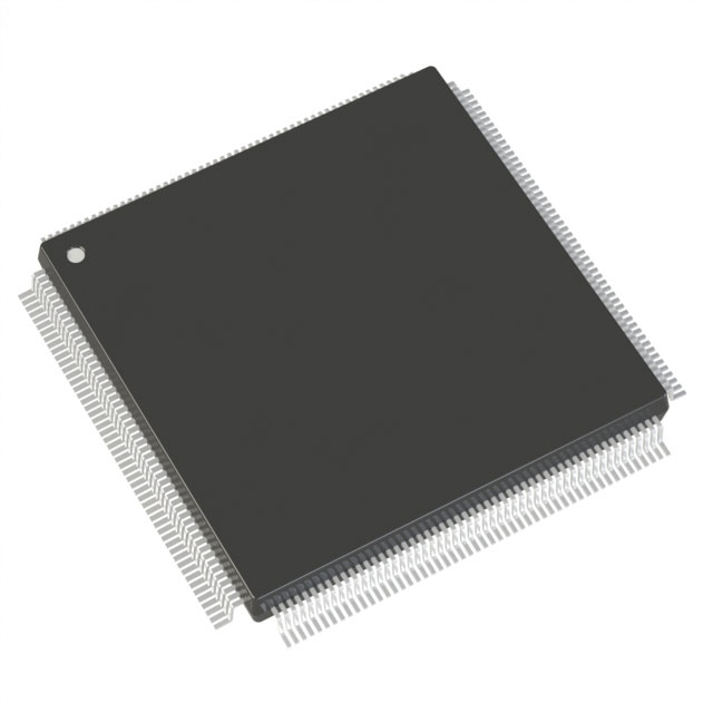
AX500-2FGG484I
| Part Description |
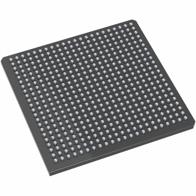
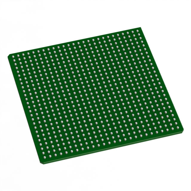
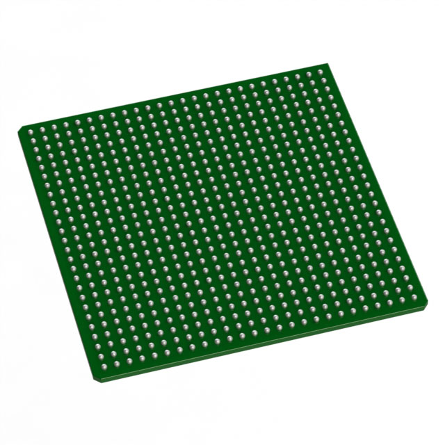
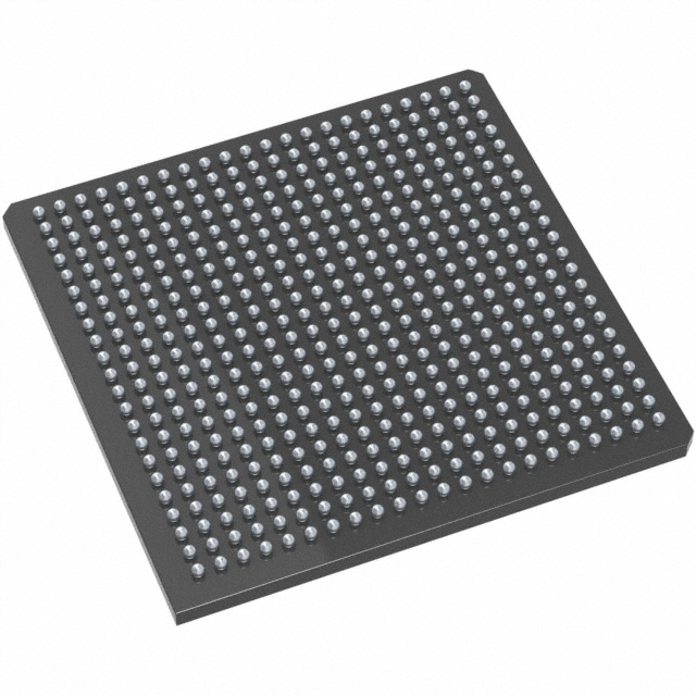
Axcelerator Field Programmable Gate Array (FPGA) IC 317 73728 484-BGA |
|---|---|
| Quantity | 1,426 Available (as of October 7, 2026) |
| Product Category | Field Programmable Gate Array (FPGA) |
|---|---|
| Manufacturer | Microchip Technology |
| Manufacturing Status | Active |
| Manufacturer Standard Lead Time | 52 Weeks |
| Datasheet |
Specifications & Environmental
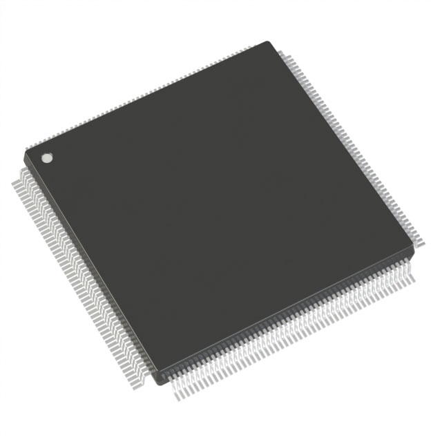
| Device Package | 484-FPBGA (23x23) | Grade | Industrial | Operating Temperature | -40°C – 85°C | ||
|---|---|---|---|---|---|---|---|
| Package / Case | 484-BGA | Number of I/O | 317 | Voltage | 1.425 V - 1.575 V | ||
| Mounting Method | Surface Mount | RoHS Compliance | ROHS3 Compliant | REACH Compliance | REACH Unaffected | ||
| Moisture Sensitivity Level | 3 (168 Hours) | Number of LABs/CLBs | 8064 | Number of Logic Elements/Cells | 8064 | ||
| Number of Gates | 500000 | ECCN | 3A991D | HTS Code | 8542.39.0001 | ||
| Qualification | N/A | Total RAM Bits | 73728 |
Overview of AX500-2FGG484I – Axcelerator FPGA, 500k gates, 484-BGA
The AX500-2FGG484I is an Axcelerator field-programmable gate array (FPGA) from Microchip Technology, built on the AX architecture and a CMOS antifuse process. This nonvolatile single-chip FPGA delivers a combination of high internal performance, embedded memory and flexible I/O suitable for industrial embedded designs.
With 500,000 equivalent system gates, 317 user I/Os and an industrial operating range, the device is aimed at applications requiring deterministic timing, on-chip FIFOs and mixed-voltage I/O support while operating between −40°C and 85°C.
Key Features
- Core Architecture — AX architecture implemented in a CMOS antifuse process (0.15 µm, seven metal layers) providing a single-chip, nonvolatile solution.
- Logic Capacity — 500,000 equivalent system gates and 8,064 logic elements for complex logic integration.
- Embedded Memory — 73,728 bits of on-chip RAM (approximately 0.074 Mbits) with variable-aspect RAM blocks and embedded FIFO control logic.
- High Performance — Family-level performance characteristics include 350+ MHz system performance and 500+ MHz internal performance, plus embedded PLLs with frequency synthesis capabilities (datasheet family values).
- I/O Flexibility — 317 user I/Os with bank-selectable, mixed-voltage operation (1.5 V, 1.8 V, 2.5 V, 3.3 V) and support for differential standards including LVDS; high-speed LVDS capable I/Os (700 Mb/s family-level figure).
- Power and Voltage — Core supply range specified at 1.425 V to 1.575 V for low-voltage operation.
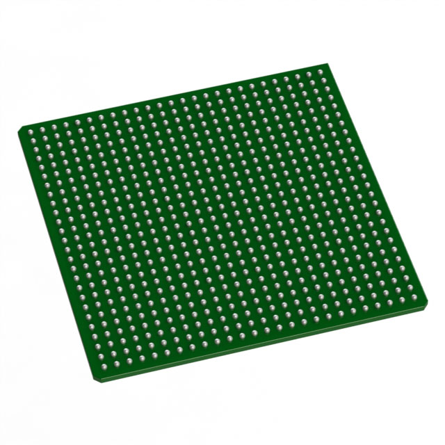
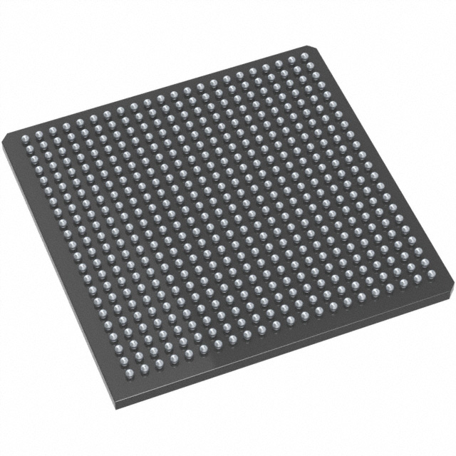
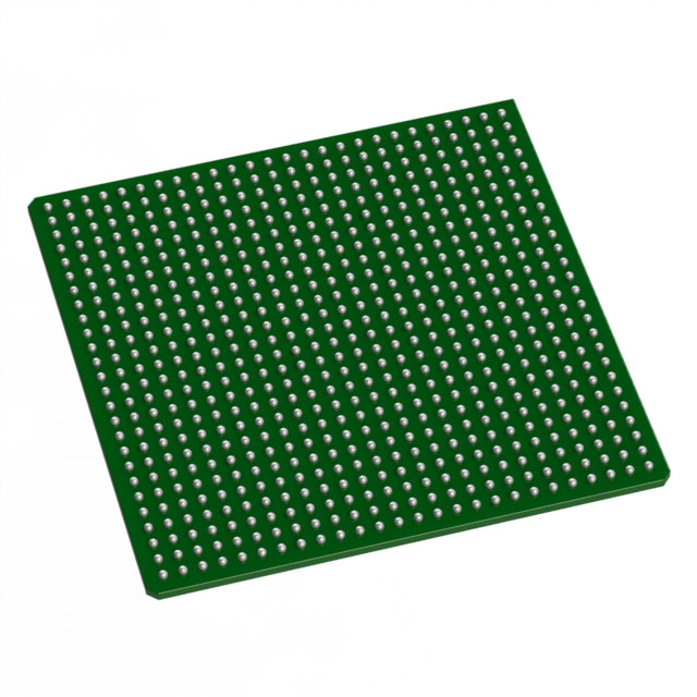
- Package and Mounting — 484-ball fine-pitch BGA (484-FPBGA, 23 × 23) surface-mount package for compact board integration.
- Industrial Grade Reliability — Rated for operation from −40°C to 85°C and RoHS compliant.
- Security and Test — FuseLock™ programming technology to protect designs and IEEE 1149.1 (JTAG) boundary-scan testing support (family-level features).
Typical Applications
- Industrial Control — Implement complex control logic, I/O aggregation and deterministic timing for factory automation and motion-control systems.
- Data Acquisition and Transport — Use embedded FIFOs and flexible I/O standards to buffer and route high-speed sensor or telemetry data streams.
- Communications Interfaces — Implement protocol bridging, SERDES-adjacent interfacing and LVDS-based links leveraging the device’s high-speed I/O capabilities.
- Embedded Systems — Integrate glue logic, bus interfaces and custom processing blocks while minimizing external components thanks to on-chip memory and logic density.
Unique Advantages
- Nonvolatile Single-Chip Solution: Antifuse-based architecture provides a nonvolatile FPGA that eliminates external configuration memory and simplifies system initialization.
- High Logic Density: 500,000 equivalent gates and 8,064 logic elements allow consolidation of multiple functions into one device, reducing PCB BOM and routing complexity.
- Flexible, Mixed-Voltage I/O: Bank-selectable I/O with multi-standard support (1.5 V–3.3 V) enables easy interfacing to a range of legacy and modern peripherals.
- Embedded Memory and FIFO Support: 73,728 bits of on-chip RAM with embedded FIFO control logic supports buffering and data-width adaptation without external RAM.
- Industrial Temperature Range: Rated for −40°C to 85°C operation to meet industrial deployment requirements.
- Security and Testability: FuseLock programming technology and JTAG boundary-scan support protect IP and simplify board-level test.
Why Choose AX500-2FGG484I?
The AX500-2FGG484I positions itself as a robust, industrial-grade FPGA option for designs that require substantial logic capacity, on-chip memory and flexible high-speed I/O in a compact BGA package. Its antifuse-based, nonvolatile nature and family-level performance characteristics make it suitable for systems that demand deterministic behavior and reliable startup without external configuration.
This device is well suited to engineering teams building industrial embedded systems, communication interfaces or data acquisition platforms that benefit from consolidated logic, embedded FIFOs and mixed-voltage I/O support while operating across an industrial temperature range.
Request a quote or submit an RFQ to obtain pricing and lead-time information for the AX500-2FGG484I.





















Date Founded: 1989
Headquarters: Chandler, Arizona, USA
Employees: 22,000+
Revenue: $8.349 Billion
Certifications and Memberships: ISO9001:2015, IATF16949:2016, AS 9100D




