
AX500-2PQ208I
| Part Description |
Axcelerator Field Programmable Gate Array (FPGA) IC 115 73728 208-BFQFP |
|---|---|
| Quantity | 1,594 Available (as of June 15, 2026) |

| Product Category | Field Programmable Gate Array (FPGA) |
|---|---|
| Manufacturer | Microchip Technology |
| Manufacturing Status | Obsolete |
| Manufacturer Standard Lead Time | Contact Us |
| Datasheet |
Specifications & Environmental
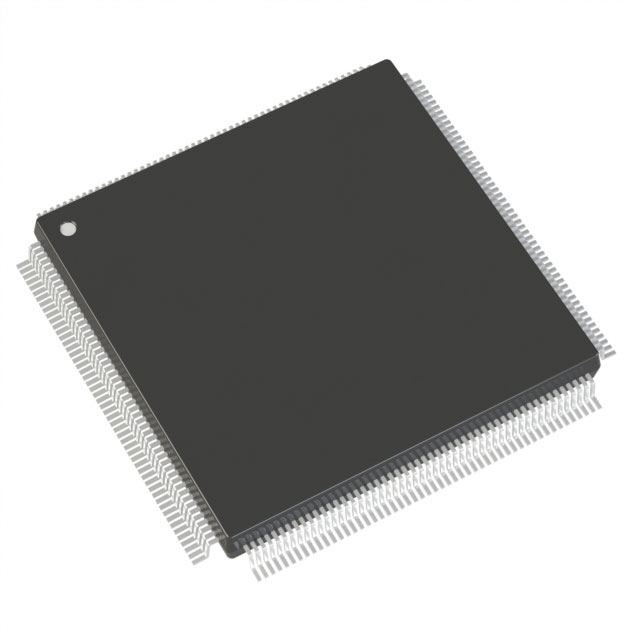
| Device Package | 208-PQFP (28x28) | Grade | Industrial | Operating Temperature | -40°C – 85°C | ||
|---|---|---|---|---|---|---|---|
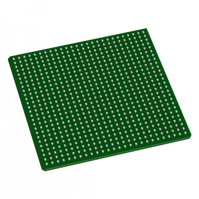
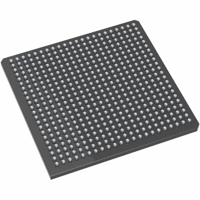
| Package / Case | 208-BFQFP | Number of I/O | 115 | Voltage | 1.425 V - 1.575 V | ||
| Mounting Method | Surface Mount | RoHS Compliance | RoHS non-compliant | REACH Compliance | REACH Unaffected | ||
| Moisture Sensitivity Level | 3 (168 Hours) | Number of LABs/CLBs | 8064 | Number of Logic Elements/Cells | 8064 | ||
| Number of Gates | 500000 | ECCN | 3A991D | HTS Code | 8542.39.0001 | ||
| Qualification | N/A | Total RAM Bits | 73728 |
Overview of AX500-2PQ208I – Axcelerator FPGA, 115 I/O, 73,728-bit RAM, 208-BFQFP
The AX500-2PQ208I is an Axcelerator Field Programmable Gate Array (FPGA) from Microchip Technology based on the AX architecture and antifuse CMOS process. This single‑chip, nonvolatile FPGA combines deterministic timing, embedded SRAM/FIFO control logic and flexible multi‑standard I/Os for system-level designs that require performance and design security.
Targeted at industrial applications, the device offers 500,000 equivalent system gates, 8,064 logic elements and approximately 0.074 Mbits of embedded memory, delivering a compact, surface‑mount solution in a 208‑pin BFQFP package for mid-density FPGA requirements.
Key Features
- Core & Performance 500,000 equivalent system gates and 8,064 logic elements provide the programmable resources for mid-density designs. Datasheet family characteristics indicate system performance above 350 MHz and internal performance above 500 MHz.
- Memory & FIFO Approximately 73,728 bits of embedded SRAM with programmable FIFO control logic for buffering and data‑stream management in high‑throughput designs.
- I/O Flexibility 115 user I/Os on this variant with support for multi‑standard, bank‑selectable I/O operation. Family features include LVDS capable I/Os (up to 700 Mb/s) and a wide range of single‑ended and differential I/O standards.
- Power & Voltage Core voltage specified at approximately 1.5 V with an operating supply window of 1.425 V to 1.575 V, enabling low‑power core operation consistent with the Axcelerator family.
- Package & Mounting 208‑BFQFP (supplier device package 208‑PQFP, 28 × 28) surface‑mount package suitable for streamlined PCB assembly and board‑level integration.
- Industrial Temperature Grade Rated for operation from −40 °C to 85 °C, meeting industrial temperature requirements for deployed systems.
- Security & Reliability Antifuse, single‑chip nonvolatile implementation and FuseLock™ programming technology (family feature) for enhanced design security and protection against reverse engineering.
- Manufacturing Technology Built on advanced 0.15 μm CMOS antifuse process with seven metal layers (family characteristic) to support higher routing density and performance.
- Standards & Testability Boundary‑scan testing compliant with IEEE 1149.1 (JTAG) and unique in‑system diagnostic/debug capability (family feature) to simplify development and manufacturing test.
Typical Applications
- Industrial Control Implement real‑time control logic, motor control interfaces and deterministic timing blocks using the device’s logic elements, embedded memory and PLL resources.
- High‑Speed Data Interfaces Use LVDS‑capable I/Os and embedded FIFO control to manage high‑throughput serial links and board‑to‑board data channels.
- Communication and Networking Subsystems Leverage the device’s programmable I/O standards and embedded memory for protocol bridging, packet buffering and timing‑sensitive datapaths.
- Secure, Nonvolatile Implementations Deploy a single‑chip nonvolatile solution where design security and in‑field robustness are required, using antifuse programming and FuseLock protection.
Unique Advantages
- Deterministic, Nonvolatile Platform: Antifuse-based, single‑chip nonvolatile architecture ensures fixed, repeatable timing and inherent configuration protection across power cycles.
- Mid‑Density Integration: 8,064 logic elements and 500,000 gates pack significant programmable logic into a compact footprint, reducing the need for external glue logic.
- Embedded Memory with FIFO Support: On‑chip SRAM blocks and programmable FIFO control simplify buffering and dataflow management without external memory components.
- Flexible I/O Options: Multi‑standard, bank‑selectable I/Os and LVDS capability support mixed‑voltage interfaces and high‑speed links on the same device.
- Industrial Rating and Surface‑Mount Packaging: Industrial temperature rating (−40 °C to 85 °C) and 208‑pin BFQFP surface‑mount package ease deployment in ruggedized and space‑constrained boards.
- Proven Process Technology: Manufactured on a 0.15 μm CMOS antifuse process with seven metal layers to deliver reliable routing density and performance.
Why Choose AX500-2PQ208I?
The AX500-2PQ208I positions itself as a robust, mid‑density Axcelerator FPGA offering a balance of programmable logic capacity, embedded memory and flexible I/O in an industrial‑rated, surface‑mount package. Its antifuse nonvolatile architecture and FuseLock programming support designs that prioritize security, deterministic timing and long‑term configuration stability.
This variant is well suited for engineers building industrial control systems, high‑speed data interfaces and secure embedded subsystems who need a compact FPGA with on‑chip SRAM/FIFO support, LVDS capable I/Os and proven manufacturing technology from Microchip.
Request a quote or submit a purchase inquiry for AX500-2PQ208I today referencing the exact part number to begin procurement or volume planning.


Date Founded: 1989
Headquarters: Chandler, Arizona, USA
Employees: 22,000+
Revenue: $8.349 Billion
Certifications and Memberships: ISO9001:2015, IATF16949:2016, AS 9100D


