
AX500-2PQG208I
| Part Description |
Axcelerator Field Programmable Gate Array (FPGA) IC 115 73728 208-BFQFP |
|---|---|
| Quantity | 1,406 Available (as of June 10, 2026) |

| Product Category | Field Programmable Gate Array (FPGA) |
|---|---|
| Manufacturer | Microchip Technology |
| Manufacturing Status | Active |
| Manufacturer Standard Lead Time | 8 Weeks |
| Datasheet |
Specifications & Environmental
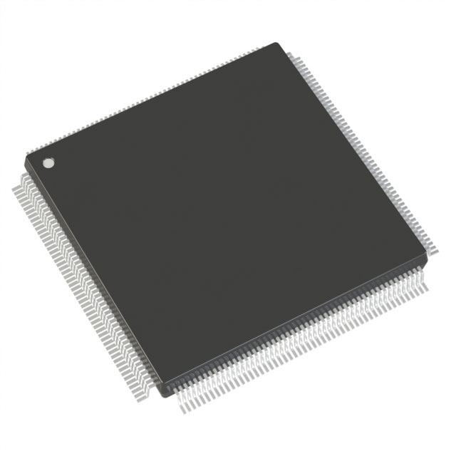
| Device Package | 208-PQFP (28x28) | Grade | Industrial | Operating Temperature | -40°C – 85°C | ||
|---|---|---|---|---|---|---|---|
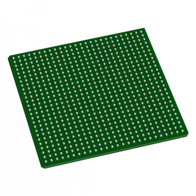
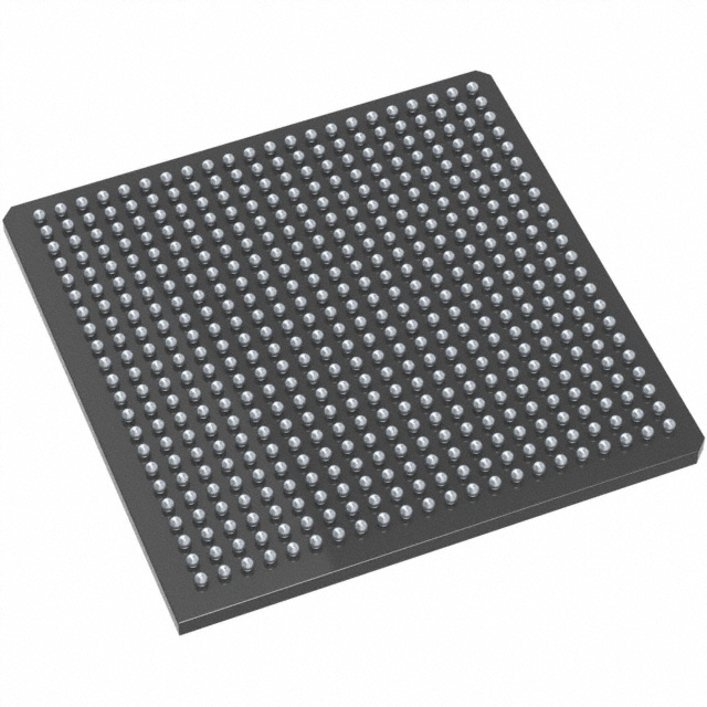
| Package / Case | 208-BFQFP | Number of I/O | 115 | Voltage | 1.425 V - 1.575 V | ||
| Mounting Method | Surface Mount | RoHS Compliance | ROHS3 Compliant | REACH Compliance | REACH Unaffected | ||
| Moisture Sensitivity Level | 3 (168 Hours) | Number of LABs/CLBs | 8064 | Number of Logic Elements/Cells | 8064 | ||
| Number of Gates | 500000 | ECCN | 3A991D | HTS Code | 8542.39.0001 | ||
| Qualification | N/A | Total RAM Bits | 73728 |
Overview of AX500-2PQG208I – Axcelerator Field Programmable Gate Array (FPGA) IC 115 73728 208-BFQFP
The AX500-2PQG208I is an Axcelerator antifuse FPGA from Microchip Technology built on the AX architecture. This single-chip, nonvolatile FPGA delivers 500,000 equivalent system gates with 8,064 logic elements and approximately 73,728 bits of embedded RAM, packaged in a 208‑lead BFQFP for surface-mount applications.
Designed for industrial-grade applications (–40 °C to 85 °C), the device combines high internal performance with flexible I/O and embedded system resources such as PLLs, segmentable clocks and FIFO control logic, making it suitable for demanding embedded, communications and industrial control designs.
Key Features
- Core Performance 500,000 equivalent system gates and 8,064 logic elements provide substantial programmable logic capacity for mid-density designs.
- Embedded Memory Approximately 73,728 bits of on-chip RAM with variable-aspect 4,608-bit RAM blocks and programmable FIFO control logic for efficient buffering and data path implementation.
- I/O Flexibility 115 user I/Os with support for multi-standard operation; family-level I/O capabilities include LVDS (700 Mb/s capable) and a variety of single-ended and differential standards.
- Clocking and Timing Segmentable clock resources and on-chip PLLs offer precise clock management; family specifications cite system performance above 350 MHz and internal performance above 500 MHz.
- Security and Test FuseLock™ programming technology for protection against reverse engineering and design theft, plus IEEE 1149.1 (JTAG) boundary-scan support for board-level testing.
- Packaging and Mounting 208‑lead BFQFP (supplier device package: 208‑PQFP 28×28) in a surface-mount form factor for compact board integration.
- Power Core supply operating range of 1.425 V to 1.575 V (nominal 1.5 V) for low-voltage core operation.
- Industrial Temperature Grade Rated for –40 °C to 85 °C operation to meet industrial environmental requirements.
- Compliance RoHS compliant.
Typical Applications
- Industrial Control and Automation Use the AX500-2PQG208I for controller logic, custom I/O handling and deterministic timing in equipment that requires industrial operating temperature range.
- High-Speed Serial and Interface Processing Implement LVDS-capable interfaces and embedded FIFO memory to manage high-throughput data paths and protocol bridging.
- Embedded Systems and Communications Deploy as a mid-density programmable fabric for protocol processing, packet buffering and custom hardware acceleration using on-chip RAM and PLLs.
- Secure, Single-Chip Solutions Leverage the antifuse, nonvolatile programming and FuseLock technology for designs requiring one-time programmable, secure hardware implementations.
Unique Advantages
- Nonvolatile, Single-Chip Implementation: Antifuse-based design provides a single, nonvolatile FPGA solution that eliminates the need for external configuration memory.
- Mixed-Voltage, Bank-Selectable I/Os: Flexible I/O bank configuration supports multiple voltage standards for heterogeneous system interfaces.
- Deterministic Timing and High Internal Performance: Segmentable clocks, embedded PLLs and documented internal performance figures support designs that need predictable timing.
- Embedded FIFO and RAM Resources: On-chip memory blocks and FIFO control logic simplify buffering and data-width adaptation without large external memory.
- Industrial Temperature Operation: Specified operation from –40 °C to 85 °C for deployment in industrial environments.
- Design Protection and Testability: FuseLock programming technology plus JTAG boundary-scan enable secure production devices and board-level test strategies.
Why Choose AX500-2PQG208I?
The AX500-2PQG208I blends substantial mid-range logic capacity and embedded memory with flexible, high-speed I/O and industrial temperature operation. Its antifuse, single-chip architecture provides a nonvolatile, secure implementation path for designs that require long-term reliability and design protection.
This device is well suited to engineers building industrial controllers, communications interfaces, and embedded systems that need deterministic timing, integrated FIFO/memory resources, and a compact 208‑lead BFQFP package. Backed by Microchip’s Axcelerator family features and on-chip PLL/clocking resources, the AX500-2PQG208I offers a pragmatic balance of performance, integration and system-level flexibility.
Request a quote or submit a request for availability and lead time to evaluate the AX500-2PQG208I for your next design project.


Date Founded: 1989
Headquarters: Chandler, Arizona, USA
Employees: 22,000+
Revenue: $8.349 Billion
Certifications and Memberships: ISO9001:2015, IATF16949:2016, AS 9100D


