
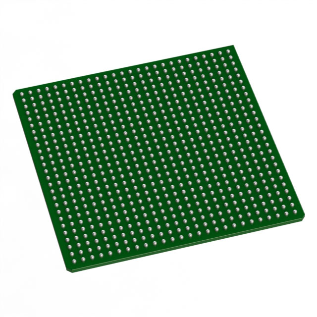
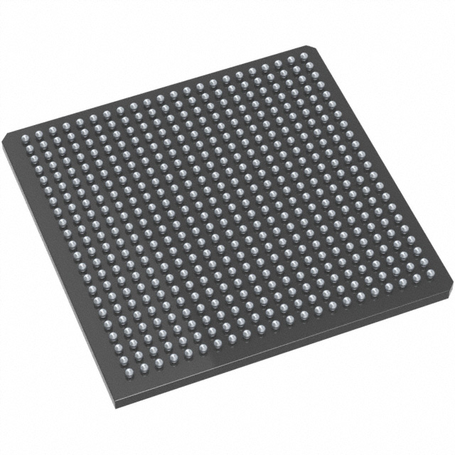
AX500-FGG676I
| Part Description |
Axcelerator Field Programmable Gate Array (FPGA) IC 336 73728 676-BGA |
|---|---|
| Quantity | 126 Available (as of June 15, 2026) |
| Product Category | Field Programmable Gate Array (FPGA) |
|---|---|
| Manufacturer | Microchip Technology |
| Manufacturing Status | Active |
| Manufacturer Standard Lead Time | 52 Weeks |
| Datasheet |
Specifications & Environmental
| Device Package | 676-FBGA (27x27) | Grade | Industrial | Operating Temperature | -40°C – 85°C | ||
|---|---|---|---|---|---|---|---|
| Package / Case | 676-BGA | Number of I/O | 336 | Voltage | 1.425 V - 1.575 V | ||
| Mounting Method | Surface Mount | RoHS Compliance | ROHS3 Compliant | REACH Compliance | REACH Unaffected | ||
| Moisture Sensitivity Level | 3 (168 Hours) | Number of LABs/CLBs | 8064 | Number of Logic Elements/Cells | 8064 | ||
| Number of Gates | 500000 | ECCN | 3A991D | HTS Code | 8542.39.0001 | ||
| Qualification | N/A | Total RAM Bits | 73728 |
Overview of AX500-FGG676I – Axcelerator Field Programmable Gate Array (FPGA) IC 336 73728 676-BGA
The AX500-FGG676I is an Axcelerator-series antifuse FPGA from Microchip Technology based on the AX architecture. It combines high-density logic, embedded SRAM/FIFO resources and flexible I/O to support performance-focused and security-conscious embedded designs.
Targeted at industrial applications, the device provides a 676‑FBGA (27×27) package, 336 user I/Os and an operating range of -40 °C to 85 °C, with a core supply window of 1.425 V to 1.575 V. On-chip programming and built-in diagnostic capabilities support long-term deployment and design protection.
Key Features
- Core Capacity — Approximately 500,000 gates and 8,064 logic elements provide mid-range programmable capacity for complex control and data-path logic.
- Embedded Memory — 73,728 bits of on-chip RAM (approximately 0.074 Mbits) with embedded FIFO control logic for buffering and streaming applications.
- I/O Flexibility — 336 user I/Os with bank-selectable, multi‑standard support across the Axcelerator family, including single-ended and differential standards and LVDS-capable interfaces.
- Packaging & Mounting — 676‑BGA package (supplier package: 676‑FBGA, 27×27) with surface-mount mounting type suitable for compact board designs.
- Power & Voltage — Core supply range of 1.425 V to 1.575 V (1.5 V core operation cited), enabling low‑voltage core operation.
- Performance & Timing Resources — AX architecture features segmentable clocks, embedded PLLs (14–200 MHz input range, synthesis up to 1 GHz) and deterministic timing controls for high-performance designs.
- Security & Test — FuseLock programming technology to protect against reverse engineering and IEEE 1149.1 JTAG boundary-scan support for board-level testing.
- Environmental Rating — Industrial-grade operation with a temperature rating from -40 °C to 85 °C; RoHS compliant.
Typical Applications
- Industrial Control — Implement custom motor control logic, sensor interfacing and factory automation functions that require deterministic timing and industrial temperature tolerance.
- High-Speed Data Interfaces — Use embedded FIFOs and LVDS-capable I/Os for protocol bridging, data acquisition front-ends and high-throughput serial links.
- Secure Embedded Systems — Leverage FuseLock programming and single-chip nonvolatile antifuse architecture for designs where design protection and reliability are priorities.
- Buffering and FIFO Management — Built-in RAM blocks with programmable FIFO control logic simplify streaming data buffering and handshaking functions in real-time systems.
Unique Advantages
- Mid-Range Logic Density with Practical I/O Count — 8,064 logic elements and 336 I/Os deliver balanced capability for control-rich and interface-heavy designs without excessive board-level complexity.
- On-Chip Memory and FIFO Support — Approximately 0.074 Mbits of embedded memory plus configurable FIFO logic reduce BOM and external memory dependencies for many buffering tasks.
- Deterministic Timing and PLL Flexibility — Segmentable clocks and embedded PLLs with wide input and synthesis ranges simplify clocking strategies across mixed-rate subsystems.
- Design Protection Built-In — FuseLock programming technology enhances IP protection against reverse engineering for sensitive applications.
- Industrial Temperature Range — Rated for -40 °C to 85 °C to meet many industrial deployment requirements.
- RoHS Compliant — Meets RoHS requirements for lead-free assembly and environmental compliance.
Why Choose AX500-FGG676I?
The AX500-FGG676I positions itself as a versatile antifuse FPGA for designers who need a combination of mid-level logic capacity, flexible high‑speed I/O and on-chip memory with FIFO capabilities. Its AX architecture provides the timing resources, embedded PLLs and security features to support industrial and performance-oriented applications while maintaining a compact 676‑FBGA footprint.
For teams building secure, deterministic embedded systems—especially where on-chip memory, reliable clocking and I/O versatility matter—the AX500-FGG676I offers a balanced, factory-tested platform backed by Microchip’s Axcelerator family features.
If you would like pricing, availability or a formal quote for the AX500-FGG676I, please request a quote or submit your requirements and a sales specialist will respond promptly.


Date Founded: 1989
Headquarters: Chandler, Arizona, USA
Employees: 22,000+
Revenue: $8.349 Billion
Certifications and Memberships: ISO9001:2015, IATF16949:2016, AS 9100D


