
AX500-FGG676M
| Part Description |
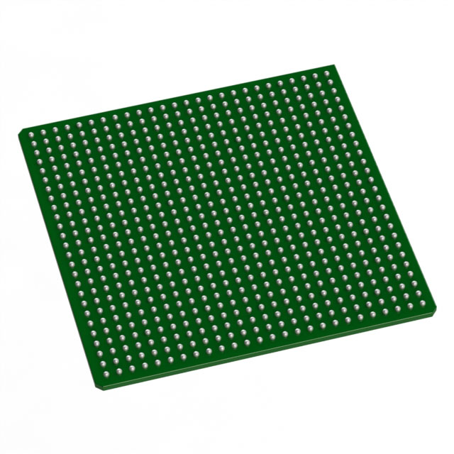
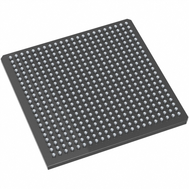
Axcelerator Field Programmable Gate Array (FPGA) IC 336 73728 676-BGA |
|---|---|
| Quantity | 1,541 Available (as of October 8, 2026) |
| Product Category | Field Programmable Gate Array (FPGA) |
|---|---|
| Manufacturer | Microchip Technology |
| Manufacturing Status | Active |
| Manufacturer Standard Lead Time | 52 Weeks |
| Datasheet |
Specifications & Environmental
| Device Package | 676-FBGA (27x27) | Grade | Military | Operating Temperature | -55°C – 125°C | ||
|---|---|---|---|---|---|---|---|
| Package / Case | 676-BGA | Number of I/O | 336 | Voltage | 1.425 V - 1.575 V | ||
| Mounting Method | Surface Mount | RoHS Compliance | ROHS3 Compliant | REACH Compliance | REACH Unaffected | ||
| Moisture Sensitivity Level | 3 (168 Hours) | Number of LABs/CLBs | 8064 | Number of Logic Elements/Cells | 8064 | ||
| Number of Gates | 500000 | ECCN | 3A001A2C | HTS Code | 8542.39.0001 | ||
| Qualification | N/A | Total RAM Bits | 73728 |
Overview of AX500-FGG676M – Axcelerator Field Programmable Gate Array (FPGA) IC 336 73728 676-BGA
The AX500-FGG676M is an Axcelerator family antifuse FPGA optimized for secure, high-performance system integration. Based on Microchip's AX architecture, it delivers a single-chip nonvolatile solution with on-chip SRAM, embedded FIFO control logic and segmentable clock resources for demanding digital designs.
This device targets applications that require deterministic timing, hardware-level design security and high-speed I/O. Key value propositions include multi-MHz internal performance, integrated memory and flexible I/O configurability in a 676-FBGA package suitable for military-grade environments.
Key Features
- Core Capacity – Approximately 500,000 equivalent system gates with 8,064 logic elements (cells) to implement complex logic and control functions.
- Embedded Memory – 73,728 total RAM bits of on-chip SRAM with variable-aspect 4,608‑bit RAM blocks and embedded FIFO control logic for buffering and packet handling.
- High-Performance Timing – Family-level performance indicators include 350+ MHz system performance and 500+ MHz internal performance; deterministic, user-controllable timing and segmentable clock resources are provided.
- Programmable I/O – 336 user I/Os with support for mixed-voltage operation and high-speed differential standards (LVDS, LVPECL) including 700 Mb/s LVDS-capable I/Os and bank-selectable I/O banks.
- On-Chip PLLs – Embedded PLLs with 14–200 MHz input range and frequency synthesis capabilities to support system clocking up to 1 GHz (family-level specification).
- Security and Nonvolatile Programming – Antifuse, single-chip nonvolatile architecture with FuseLock programming technology to protect against reverse engineering and design theft.
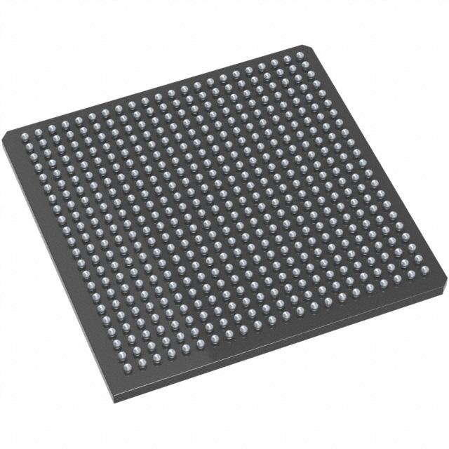
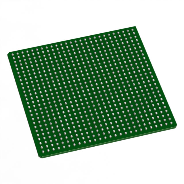
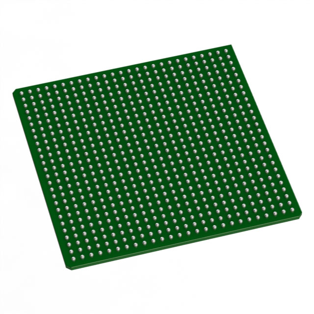
- Package and Mounting – 676‑FBGA (27 × 27) surface-mount package (676‑BGA case) suitable for compact board layouts.
- Power and Temperature – Core supply range 1.425 V to 1.575 V; rated operating temperature −55 °C to 125 °C and classified as Military grade.
- Standards and Testability – Boundary-scan testing compliant with IEEE 1149.1 (JTAG) and unique in-system diagnostic and debug capability with Microchip Silicon Explorer II (family feature).
- Environmental – RoHS compliant.
Typical Applications
- Defense and Military Systems – Military-grade operating temperature and robust nonvolatile antifuse programming make this device suitable for defense electronics requiring secure, long-term operation.
- High-Speed Data Transport – Embedded FIFOs, high-performance internal timing and 700 Mb/s-capable LVDS I/Os enable deployment in data multiplexing, backplane bridging and SERDES-adjacent subsystems.
- Telecommunications Infrastructure – Deterministic timing, on-chip RAM and PLL frequency synthesis support packet buffering, framing and clock-domain crossing in telecom line cards and routers.
- Secure System Control – Nonvolatile antifuse programming and FuseLock protection suit applications where design confidentiality and tamper resistance are required.
Unique Advantages
- Nonvolatile, One-Time Programmable Security: Antifuse programming with FuseLock protects intellectual property and prevents reverse engineering.
- Integrated Memory and FIFO Support: 73,728 bits of embedded SRAM with programmable FIFO control logic reduces external memory requirements and simplifies buffering designs.
- High I/O Count and Flexibility: 336 user I/Os with mixed-voltage and differential-standard support allow direct interfacing to multiple system buses and high-speed links.
- Deterministic Performance: Segmentable clocks, embedded PLLs and user-controllable timing support precision timing and reliable synchronous design.
- Military-Grade Thermal Range: −55 °C to 125 °C rating supports deployment in harsh-environment systems.
- Compact System Footprint: 676-FBGA package provides high pin density for complex designs while enabling space-efficient board layouts.
Why Choose AX500-FGG676M?
The AX500-FGG676M brings together antifuse nonvolatile programming, a high logic-element count and integrated SRAM into a single, military-grade FPGA package. Its blend of deterministic timing, embedded FIFO capability and flexible, high-speed I/O makes it well suited for secure, high-performance applications where long-term reliability and design protection are priorities.
Designers and system integrators will find the AX500-FGG676M appropriate for compact, rugged deployments that require reduced external BOM, stable timing behavior and hardware-level IP protection, backed by Axcelerator family architecture and Microchip's in-system diagnostic features.
Request a quote or submit a price inquiry to evaluate the AX500-FGG676M for your next secure, high-performance FPGA design.























Date Founded: 1989
Headquarters: Chandler, Arizona, USA
Employees: 22,000+
Revenue: $8.349 Billion
Certifications and Memberships: ISO9001:2015, IATF16949:2016, AS 9100D




