
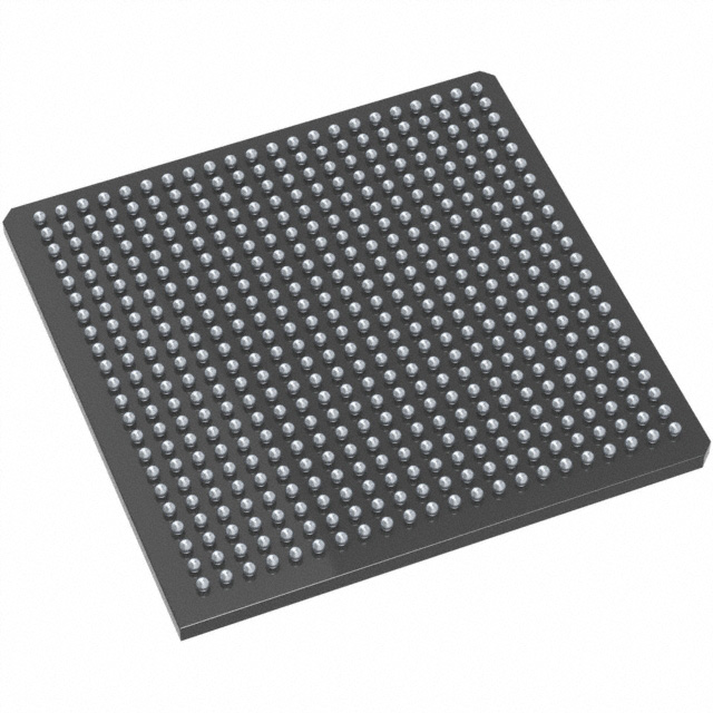
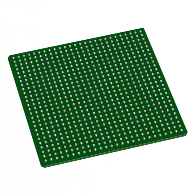
AX500-FGG484I
| Part Description |
Axcelerator Field Programmable Gate Array (FPGA) IC 317 73728 484-BGA |
|---|---|
| Quantity | 1,054 Available (as of June 15, 2026) |
| Product Category | Field Programmable Gate Array (FPGA) |
|---|---|
| Manufacturer | Microchip Technology |
| Manufacturing Status | Active |
| Manufacturer Standard Lead Time | 8 Weeks |
| Datasheet |
Specifications & Environmental
| Device Package | 484-FPBGA (23x23) | Grade | Industrial | Operating Temperature | -40°C – 85°C | ||
|---|---|---|---|---|---|---|---|
| Package / Case | 484-BGA | Number of I/O | 317 | Voltage | 1.425 V - 1.575 V | ||
| Mounting Method | Surface Mount | RoHS Compliance | ROHS3 Compliant | REACH Compliance | REACH Unaffected | ||
| Moisture Sensitivity Level | 3 (168 Hours) | Number of LABs/CLBs | 8064 | Number of Logic Elements/Cells | 8064 | ||
| Number of Gates | 500000 | ECCN | 3A991D | HTS Code | 8542.39.0001 | ||
| Qualification | N/A | Total RAM Bits | 73728 |
Overview of AX500-FGG484I – Axcelerator Field Programmable Gate Array (FPGA) IC, 500,000 gates, 484-BGA
The AX500-FGG484I is an Axcelerator antifuse FPGA built on Microchip’s AX architecture. This single-chip, nonvolatile FPGA combines high internal performance with deterministic timing and on-chip embedded SRAM/FIFO control for embedded and industrial-class designs.
Designed for systems that require high-speed I/O, embedded memory and robust clocking, the AX500-FGG484I delivers substantial logic capacity and flexible mixed-voltage I/O while operating across an industrial temperature range.
Key Features
- Core architecture – Antifuse-based Axcelerator AX architecture providing a nonvolatile single-chip solution with deterministic and user-controllable timing.
- Logic capacity – 500,000 equivalent system gates and 8,064 logic elements for substantial on-chip logic integration.
- Embedded memory – 73,728 bits of on-chip RAM/FIFO (≈0.074 Mbits) with variable-aspect RAM blocks and programmable FIFO control logic for buffering and data staging.
- I/O flexibility – 317 user I/Os with bank-selectable, mixed-voltage operation and support for single-ended and differential standards; LVDS-capable I/Os rated to 700 Mb/s.
- Clocking and PLLs – Segmentable clock resources and embedded PLLs (14–200 MHz input range, frequency synthesis up to 1 GHz) for high-performance, deterministic system timing.
- Packaging and mounting – 484-ball FPBGA package (23 × 23) designed for surface-mount assembly; industrial-grade operating temperature from −40 °C to 85 °C.
- Power – Core supply voltage specified 1.425 V to 1.575 V for consistent low-voltage operation.
- Security and test – FuseLock™ programming technology to protect against reverse engineering and built-in boundary-scan (IEEE 1149.1) for test access; in-system diagnostic and debug capability with Microchip Silicon Explorer II.
- Standards and configurability – Support for a wide set of I/O standards, programmable slew rates, drive strengths, input delays and weak pull-up/pull-down circuits for board-level signal integrity tuning.
- Compliance – RoHS-compliant for environmentally restricted applications.
Typical Applications
- High-speed data interfaces – LVDS-capable I/Os and embedded FIFO memory make this device suitable for data aggregation, protocol bridging and other high-throughput I/O functions.
- Industrial control and automation – Industrial-grade temperature range and deterministic timing support control systems, motion control, and factory automation logic consolidation.
- Embedded processing and glue logic – Large logic capacity and mixed-voltage I/O banks enable custom peripheral interfacing, bus bridging and system integration tasks.
- Timing-sensitive systems – Segmentable clocks and integrated PLLs offer designers precise clocking and frequency synthesis for timing-critical designs.
Unique Advantages
- Nonvolatile single-chip solution: Antifuse programming delivers a one-time-programmable FPGA with no external configuration memory required.
- Deterministic timing and embedded PLLs: Built-in clock resources and PLLs enable repeatable, controllable timing for reliable system behavior.
- Flexible I/O and high-speed links: Bank-selectable mixed-voltage operation and LVDS-capable I/Os support diverse interface requirements and high data-rate connectivity.
- On-chip FIFO and SRAM: Programmable embedded memory and FIFO control reduce external buffer requirements and simplify system-level data handling.
- Industrial operating range: Specified for −40 °C to 85 °C, suitable for a wide range of industrial environments.
- Integrated security and test features: FuseLock programming and IEEE 1149.1 boundary-scan support help protect IP and streamline manufacturing test.
Why Choose AX500-FGG484I?
The AX500-FGG484I combines the Axcelerator AX antifuse architecture with a sizable logic fabric, embedded SRAM/FIFO, and robust clocking to address embedded and industrial designs that require deterministic timing and secure, nonvolatile configuration. Its flexible I/O, high-speed LVDS capability and industrial temperature rating make it suitable for applications that demand reliable, high-performance data handling and interface versatility.
This device is aimed at designers who need programmable logic with on-chip memory and integrated PLLs to reduce external components, simplify board-level routing and maintain precise system timing across temperature variations.
Request a quote or submit an inquiry to discuss availability, pricing and lead times for the AX500-FGG484I.


Date Founded: 1989
Headquarters: Chandler, Arizona, USA
Employees: 22,000+
Revenue: $8.349 Billion
Certifications and Memberships: ISO9001:2015, IATF16949:2016, AS 9100D


