
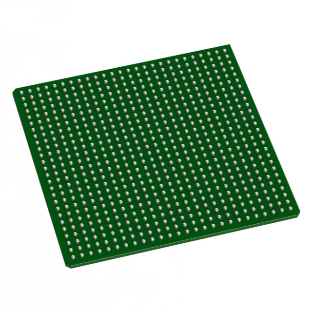
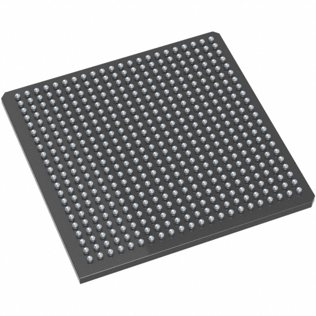
AX500-FGG484
| Part Description |
Axcelerator Field Programmable Gate Array (FPGA) IC 317 73728 484-BGA |
|---|---|
| Quantity | 170 Available (as of June 15, 2026) |

| Product Category | Field Programmable Gate Array (FPGA) |
|---|---|
| Manufacturer | Microchip Technology |
| Manufacturing Status | Active |
| Manufacturer Standard Lead Time | 52 Weeks |
| Datasheet |
Specifications & Environmental
| Device Package | 484-FPBGA (23x23) | Grade | Commercial | Operating Temperature | 0°C – 70°C | ||
|---|---|---|---|---|---|---|---|
| Package / Case | 484-BGA | Number of I/O | 317 | Voltage | 1.425 V - 1.575 V | ||
| Mounting Method | Surface Mount | RoHS Compliance | ROHS3 Compliant | REACH Compliance | REACH Unaffected | ||
| Moisture Sensitivity Level | 3 (168 Hours) | Number of LABs/CLBs | 8064 | Number of Logic Elements/Cells | 8064 | ||
| Number of Gates | 500000 | ECCN | 3A991D | HTS Code | 8542.39.0001 | ||
| Qualification | N/A | Total RAM Bits | 73728 |
Overview of AX500-FGG484 – Axcelerator FPGA, 500,000 gates, 484‑BGA
The AX500-FGG484 is an Axcelerator Field Programmable Gate Array from Microchip Technology based on the AX antifuse architecture. It provides a single‑chip, nonvolatile FPGA implementation with 500,000 equivalent system gates, 8,064 logic elements, and approximately 73.7 kbits of embedded RAM.
Designed for applications that demand deterministic timing, embedded FIFO memory and high‑speed I/O capability, the device combines 317 user I/Os, high internal performance and programmable routing in a 484‑ball fine BGA (23 × 23) surface‑mount package. The device is RoHS‑compliant and specified for commercial temperature operation.
Key Features
- Core Capacity 500,000 equivalent system gates with 8,064 logic elements (cells) to implement moderately complex custom logic and control functions.
- Embedded Memory Approximately 73.7 kbits of on‑chip RAM with variable‑aspect RAM blocks and embedded FIFO control logic for buffering and data‑path implementations.
- I/O Count & Flexibility 317 user I/Os in an 8‑bank architecture (family feature set) supporting mixed‑voltage operation and a variety of single‑ended and differential standards as documented for the Axcelerator family.
- High‑Speed I/O Capability Family‑level support for 700 Mb/s LVDS‑capable I/Os and programmable drive/slew settings to match interface requirements.
- Performance & Timing AX architecture delivers high internal performance and deterministic timing; family specifications indicate 350+ MHz system performance and 500+ MHz internal performance.
- Nonvolatile Antifuse Technology Single‑chip antifuse programming with FuseLock™ programming technology to protect design IP against reverse engineering.
- Power & Supply Core operating supply specified at 1.425 V to 1.575 V (nominal ~1.5 V) for low‑voltage core operation.
- Package & Mounting 484‑ball fine BGA (484‑FPBGA, 23 × 23) surface‑mount package for high‑density board integration in commercial applications.
- Commercial Temperature Range Specified for operation from 0 °C to 70 °C for commercial‑grade deployments.
- Standards & Test Family features include IEEE 1149.1 (JTAG) boundary‑scan support for board‑level testability.
Typical Applications
- High‑Speed Communications Use the AX500 for protocol bridging and interface aggregation where LVDS and high‑speed single/differential I/O capability is required.
- Data Buffering and Packet Processing Embedded RAM and programmable FIFO control logic allow efficient implementation of buffering, packet queueing and streaming data paths.
- Secure, Nonvolatile Logic Antifuse nonvolatile programming and FuseLock™ protection make the device suitable for designs requiring one‑time programmable hardware and IP protection.
- Custom Logic Integration Implement control, glue logic, or custom state machines in a compact BGA package while keeping board BOM low and integration high.
Unique Advantages
- Single‑Chip Nonvolatile Solution: Antifuse technology provides a persistent configuration without external configuration memory.
- Deterministic Performance: AX architecture and family timing features support predictable timing for latency‑sensitive designs.
- Built‑In FIFO and Memory: Embedded RAM blocks with FIFO control simplify data path and buffering implementations, reducing external memory needs.
- Flexible I/O Capability: High I/O count and family support for mixed‑voltage and differential standards enable a wide range of interface options on a single device.
- Compact, Surface‑Mount Packaging: 484‑ball FPBGA (23 × 23) delivers high pin density in a manufacturable surface‑mount form factor.
- Design Security: FuseLock™ programming technology helps protect intellectual property against reverse engineering and unauthorized readout.
Why Choose AX500-FGG484?
The AX500‑FGG484 brings a balanced combination of capacity, embedded memory and flexible I/O in a nonvolatile antifuse FPGA. With 500k equivalent system gates, 8,064 logic elements and approximately 73.7 kbits of embedded RAM, it addresses designs that need integrated FIFOs, deterministic timing and protected, one‑time programmable logic in a compact 484‑ball FPBGA package.
This device is well suited to commercial‑temperature applications where design security, predictable performance and on‑chip buffering reduce system complexity and BOM. Backed by Microchip’s Axcelerator family architecture and FuseLock™ programming, AX500‑FGG484 offers a robust platform for deployable, nonvolatile programmable logic solutions.
Request a quote or submit an inquiry to receive pricing and availability for AX500-FGG484. Provide your quantity and delivery requirements to get a formal quote.


Date Founded: 1989
Headquarters: Chandler, Arizona, USA
Employees: 22,000+
Revenue: $8.349 Billion
Certifications and Memberships: ISO9001:2015, IATF16949:2016, AS 9100D


