
EP1AGX20CF484C6N
| Part Description |
Arria GX Field Programmable Gate Array (FPGA) IC 230 1229184 21580 484-BBGA |
|---|---|
| Quantity | 1,897 Available (as of October 8, 2026) |

| Product Category | Field Programmable Gate Array (FPGA) |
|---|---|
| Manufacturer | Intel |
| Manufacturing Status | Obsolete |
| Manufacturer Standard Lead Time | Contact Us |
| Datasheet |
Specifications & Environmental
| Device Package | 484-FBGA (23x23) | Grade | Commercial | Operating Temperature | 0°C – 85°C | ||
|---|---|---|---|---|---|---|---|
| Package / Case | 484-BBGA | Number of I/O | 230 | Voltage | 1.15 V - 1.25 V | ||
| Mounting Method | Surface Mount | RoHS Compliance | RoHS Compliant | REACH Compliance | REACH Unaffected | ||
| Moisture Sensitivity Level | 3 (168 Hours) | Number of LABs/CLBs | 1079 | Number of Logic Elements/Cells | 21580 | ||
| Number of Gates | N/A | ECCN | 3A991D | HTS Code | 8542.39.0001 | ||
| Qualification | N/A | Total RAM Bits | 1229184 |
Overview of EP1AGX20CF484C6N – Arria GX Field Programmable Gate Array (FPGA) IC, 21,580 logic elements, 484‑BBGA
The EP1AGX20CF484C6N is an Arria GX family FPGA from Intel, delivering a mid‑range programmable logic device with integrated high‑speed serial capabilities and a dense I/O complement. The device combines approximately 21,580 logic elements, roughly 1.23 Mbits of embedded memory, and family-level transceiver and DSP capabilities aimed at applications that require serial protocol support, flexible I/O, and on‑chip memory resources.
Designed for commercial‑temperature systems, this surface‑mount FPGA is supplied for 1.15–1.25 V operation and is RoHS compliant, making it suitable for a broad range of embedded and communications designs.
Key Features
- Core capacity — Approximately 21,580 logic elements for implementing mid‑range programmable logic and control functions.
- Embedded memory — Approximately 1.23 Mbits of on‑chip RAM to support FIFOs, buffers, and local data storage.
- I/O density — 230 user I/O pins to connect multiple peripherals, memory interfaces, and high‑speed links.
- High‑speed serial support (family feature) — Arria GX family transceivers support CDR operation up to 3.125 Gbps and are targeted at protocols such as PCI Express, Gigabit Ethernet, SDI, SerialLite II, XAUI, and Serial RapidIO, enabling serial‑link designs.
- FPGA architecture features (family feature) — Includes TriMatrix memory options, dedicated DSP block support, and multiple PLLs for clocking flexibility as described in the Arria GX device handbook.
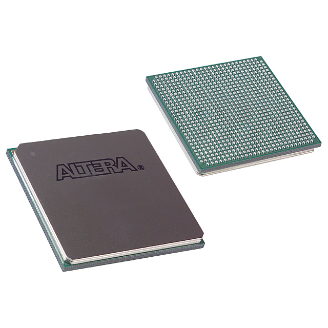
- Package and mounting — 484‑BBGA package (supplier device package: 484‑FBGA, 23×23) in a surface‑mount form factor for board‑level assembly.
- Power and temperature — Specified supply range of 1.15 V to 1.25 V and commercial operating temperature range of 0 °C to 85 °C.
- Regulatory — RoHS compliant.
Typical Applications
- High‑speed serial links — Implement protocol endpoints or bridging logic for PCIe, Gigabit Ethernet, SDI, XAUI, and similar serial interfaces using Arria GX transceiver capabilities.
- Embedded packet processing — Use on‑chip logic plus approximately 1.23 Mbits of RAM for packet buffering, packet inspection, and protocol adaptation functions.
- DSP and signal processing — Implement mid‑range DSP functions and filtering leveraging the family’s dedicated DSP resources and local memory.
- Memory interfaces and buffering — Serve as a controller or interface glue for external DDR/DDR2 memory and device‑level buffering requirements (family‑level support referenced in device handbook).
Unique Advantages
- Balanced logic and memory — Approximately 21,580 logic elements paired with ~1.23 Mbits of embedded RAM provide a balanced resource set for control, buffering, and data‑path tasks.
- High I/O count — 230 I/O pins enable connectivity to multiple peripherals, parallel buses, and serial PHYs without adding external I/O expanders.
- Serial protocol enablement — Arria GX family transceiver capabilities (CDR up to 3.125 Gbps) support a range of serial protocols, allowing designers to build high‑speed link endpoints and bridges.
- Compact board footprint — 484‑ball BGA/FBGA package in a surface‑mount form factor helps reduce overall board area for compact system designs.
- Commercial temperature rating — Specified 0 °C to 85 °C operating range aligns with a broad set of embedded and communications applications.
- RoHS compliance — Meets RoHS requirements for environmentally conscious product design and manufacturing.
Why Choose EP1AGX20CF484C6N?
The EP1AGX20CF484C6N positions itself as a practical Arria GX FPGA for designers who need mid‑range programmable logic with integrated memory and a high I/O count, combined with the Arria GX family’s high‑speed serial and DSP architecture capabilities. Its surface‑mount 484‑BBGA packaging and commercial temperature rating make it suitable for a wide range of embedded communications and signal‑processing designs.
Choose this device when your design requires a balanced mix of logic, embedded RAM, and I/O density, together with the Arria GX family-level features for serial interfaces and DSP support documented in the device handbook.
Request a quote or submit a procurement inquiry to get pricing and availability for EP1AGX20CF484C6N.
























Date Founded: 1968
Headquarters: Santa Clara, California, USA
Employees: 130,000+
Revenue: $54.23 Billion
Certifications and Memberships: ISO9001:2015, ISO14001:2015, ISO17025:2017, ISO27001:2022, ISO45001:2018, ISO50001:2018


