
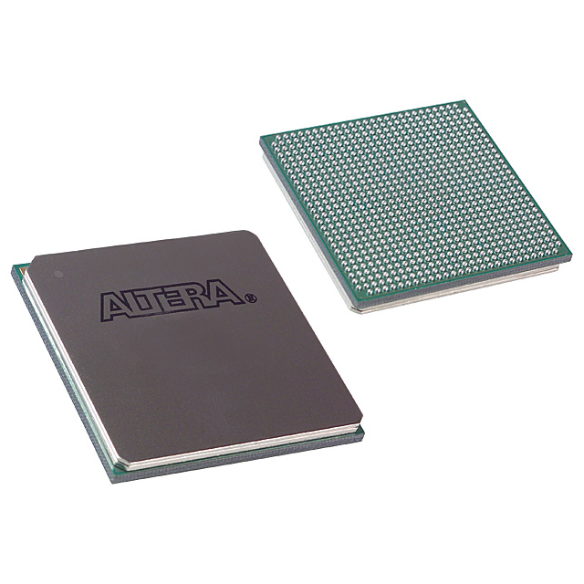
EP1AGX20CF780I6
| Part Description |
Arria GX Field Programmable Gate Array (FPGA) IC 341 1229184 21580 780-BBGA |
|---|---|
| Quantity | 573 Available (as of October 8, 2026) |

| Product Category | Field Programmable Gate Array (FPGA) |
|---|---|
| Manufacturer | Intel |
| Manufacturing Status | Obsolete |
| Manufacturer Standard Lead Time | Contact Us |
| Datasheet |
Specifications & Environmental
| Device Package | 780-FBGA (29x29) | Grade | Industrial | Operating Temperature | -40°C – 100°C | ||
|---|---|---|---|---|---|---|---|
| Package / Case | 780-BBGA | Number of I/O | 341 | Voltage | 1.15 V - 1.25 V | ||
| Mounting Method | Surface Mount | RoHS Compliance | RoHS non-compliant | REACH Compliance | REACH Unaffected | ||
| Moisture Sensitivity Level | 3 (168 Hours) | Number of LABs/CLBs | 1079 | Number of Logic Elements/Cells | 21580 | ||
| Number of Gates | N/A | ECCN | 3A991D | HTS Code | 8542.39.0001 | ||
| Qualification | N/A | Total RAM Bits | 1229184 |
Overview of EP1AGX20CF780I6 – Arria GX Field Programmable Gate Array (FPGA) IC 341 1229184 21580 780-BBGA
The EP1AGX20CF780I6 is an Intel Arria GX FPGA provided in a 780-ball BGA package. It integrates a mid-density logic array with high-speed serial transceivers and a flexible memory architecture, targeting industrial applications that require configurable logic, on-chip memory, and multi-protocol serial interfaces.
Built for systems that demand programmable processing and serial connectivity, this device combines 21,580 logic elements, approximately 1.23 Mbits of embedded memory, and up to 12 high-speed transceiver channels (series capability) to support a range of communications and signal-processing use cases.
Key Features
- Logic Capacity – 21,580 logic elements for implementing custom FPGA logic and control functions.
- On-chip Memory – Approximately 1.23 Mbits of embedded RAM for FIFOs, buffering, and local storage.
- I/O Density – 341 I/O pins to support broad interfacing needs with external devices and peripherals.
- High-Speed Transceivers – Series Arria GX transceiver architecture with multigigabit channels supporting clock-data recovery (CDR) up to 3.125 Gbps and protocol support options including PCI Express, Gigabit Ethernet, SDI, SerialLite II, XAUI, and Serial RapidIO.
- Memory Architecture (TriMatrix) – Multiple RAM block sizes enabling true dual-port memory and FIFO implementations with performance up to series-stated frequencies.
- DSP & Timing Resources – Dedicated high-speed DSP blocks for multiply and multiply-accumulate operations and up to four enhanced PLLs for clock management and phase shifting.
- Clocking – Up to 16 global clock networks and multiple regional clock networks to simplify clock distribution across designs.
- Package & Mounting – 780-BBGA package, supplier device package 780-FBGA (29×29), surface-mount mounting type for standard PCB assembly.
- Power & Operating Range – Core supply range 1.15 V to 1.25 V; industrial operating temperature range −40 °C to 100 °C.
- Environmental – RoHS compliant.
Typical Applications
- High‑speed serial communications – Implement protocol engines and bridging functions using the device’s multigigabit transceivers and CDR support for standards like PCI Express and Gigabit Ethernet.
- Video and broadcast interfaces – Support SDI transport and related video serial links using the integrated transceiver capabilities.
- Networking and interconnect – Build packet processing, aggregation, or interface bridging systems leveraging the device’s logic capacity, embedded memory, and serial protocol support.
- Signal processing and DSP – Deploy DSP blocks and dedicated RAM for FIR filters, multiply‑accumulate tasks, and real‑time data paths.
- Custom serial IP development – Create proprietary serial-based links using the transceiver Basic mode and embedded SERDES circuitry.
Unique Advantages
- Integrated multigigabit connectivity: On-device transceivers with CDR up to 3.125 Gbps reduce external SERDES requirements and simplify high-speed link implementations.
- Balanced logic and memory resources: 21,580 logic elements paired with approximately 1.23 Mbits of RAM support medium-complexity designs requiring local buffering and state storage.
- Robust clocking and DSP support: Multiple PLLs, extensive clock networks, and dedicated DSP blocks accelerate signal-processing development and clock-domain management.
- Industrial temperature range: −40 °C to 100 °C operation enables deployment in demanding environments where extended temperature performance is required.
- High I/O count in compact package: 341 I/Os in a 780-ball BGA (29×29) package provide plentiful external connectivity while keeping board area efficient.
- Standards-oriented feature set: Transceiver and SERDES features target common serial protocols, shortening time to market for communications and video applications.
Why Choose EP1AGX20CF780I6?
The EP1AGX20CF780I6 positions itself as a versatile Arria GX FPGA option for industrial designs that require a combination of moderate logic capacity, on-chip memory, and high-speed serial interfaces. Its integrated transceivers, DSP resources, and comprehensive clocking make it suitable for communications, video, and signal-processing applications where configurable hardware and protocol flexibility are important.
With a surface-mount 780-ball BGA package and RoHS compliance, this device offers a balanced platform for engineers aiming to reduce external components while maintaining the I/O and performance headroom needed for mid-range FPGA implementations.
If you would like pricing or availability information, request a quote or submit a quote inquiry and our team will respond with the next steps.























Date Founded: 1968
Headquarters: Santa Clara, California, USA
Employees: 130,000+
Revenue: $54.23 Billion
Certifications and Memberships: ISO9001:2015, ISO14001:2015, ISO17025:2017, ISO27001:2022, ISO45001:2018, ISO50001:2018


