
EP1AGX35CF484I6N
| Part Description |
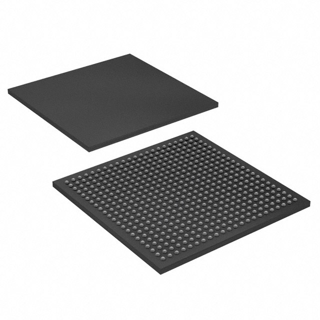
Arria GX Field Programmable Gate Array (FPGA) IC 230 1348416 33520 484-BBGA |
|---|---|
| Quantity | 139 Available (as of June 10, 2026) |

| Product Category | Field Programmable Gate Array (FPGA) |
|---|---|
| Manufacturer | Intel |
| Manufacturing Status | Obsolete |
| Manufacturer Standard Lead Time | Contact Us |
| Datasheet |
Specifications & Environmental
| Device Package | 484-FBGA (23x23) | Grade | Industrial | Operating Temperature | -40°C – 100°C | ||
|---|---|---|---|---|---|---|---|
| Package / Case | 484-BBGA | Number of I/O | 230 | Voltage | 1.15 V - 1.25 V | ||
| Mounting Method | Surface Mount | RoHS Compliance | RoHS Compliant | REACH Compliance | REACH Unaffected | ||
| Moisture Sensitivity Level | 3 (168 Hours) | Number of LABs/CLBs | 1676 | Number of Logic Elements/Cells | 33520 | ||
| Number of Gates | N/A | ECCN | 3A991D | HTS Code | 8542.39.0001 | ||
| Qualification | N/A | Total RAM Bits | 1348416 |
Overview of EP1AGX35CF484I6N – Arria GX Field Programmable Gate Array (FPGA) IC 230 1348416 33520 484-BBGA
The EP1AGX35CF484I6N is an Arria GX-series Field Programmable Gate Array (FPGA) in a 484-ball BGA package, engineered for industrial applications requiring significant logic capacity, on-chip memory and robust I/O. Built on the Arria GX device family architecture, it targets high-speed communications, video and networking subsystems and compute-intensive embedded systems that leverage programmable logic, embedded memory and transceiver-capable architectures.
This device provides a combination of 33,520 logic elements, approximately 1.35 Mbits of embedded memory, and 230 I/O pins in a compact surface-mount 484-FBGA (23×23) footprint, with an operating range and voltage compatible with industrial deployment.
Key Features
- Logic Capacity — 33,520 logic elements and 1,676 logic array blocks provide substantial programmable fabric for glue logic, protocol engines and custom datapaths.
- On‑Chip Memory — Approximately 1.35 Mbits of total RAM bits for FIFOs, buffering and local data storage.
- I/O and Package — 230 I/O pins in a 484-ball FBGA (23×23) surface-mount package for dense board-level integration and flexible interface routing.
- Voltage Supply — Core supply range of 1.15 V to 1.25 V suitable for Arria GX family logic operation.
- Industrial Temperature Rating — Specified operating temperature from -40 °C to 100 °C for demanding environments.
- Family-Level Transceiver Support — Arria GX family devices include high-speed serial transceivers with CDR support up to 3.125 Gbps and protocol support such as PCI Express, Gigabit Ethernet, SDI, SerialLite II, XAUI and Serial RapidIO (family-level feature set).
- DSP and Clocking (Family Features) — Arria GX architecture provides high-speed DSP blocks and up to four enhanced PLLs per device for advanced clocking and signal processing use cases (series-level capability).
- Compliance — RoHS compliant.
Typical Applications
- High‑Speed Networking — Implement packet processing, protocol bridging and PHY interfaces using the family’s high-speed serial transceiver support and abundant I/O.
- Video and Broadcast Systems — Support SDI and other serial video transport protocols using Arria GX transceiver features and on-chip memory for line buffering.
- Telecommunications — Use for backplane interfacing, SERDES-based links and protocol offload implementations leveraging the family’s CDR-capable transceivers.
- Embedded Signal Processing — Deploy DSP blocks and embedded memory for FIR filters, custom accelerators and real‑time data processing pipelines.
Unique Advantages
- Substantial Programmable Fabric: 33,520 logic elements and 1,676 logic array blocks enable complex custom logic and system integration on a single device, reducing external component count.
- On‑Chip Memory for Low‑Latency Designs: Approximately 1.35 Mbits of embedded RAM simplifies FIFO, buffering and local storage requirements without immediate external memory.
- Robust I/O in a Compact Package: 230 I/O in a 484-FBGA (23×23) surface-mount package supports dense board routing while maintaining industrial package robustness.
- Industrial Temperature Range: Rated for -40 °C to 100 °C, supporting deployment in temperature-challenging environments.
- Family-Level High-Speed Connectivity: Arria GX family support for up to 3.125 Gbps transceivers and common serial protocols enables rapid development of communication and video subsystems.
- Standards‑Aware Design Base: Device family architecture includes dedicated circuitry and megafunction support for common bus and memory interfaces, assisting faster design integration (series-level capability).
Why Choose EP1AGX35CF484I6N?
The EP1AGX35CF484I6N positions itself as a capable Arria GX FPGA option for engineers who need a balance of logic density, embedded memory and extensive I/O in a compact industrial‑rated BGA package. Its combination of 33,520 logic elements, roughly 1.35 Mbits of on‑chip RAM and 230 I/O pins makes it suitable for medium‑to‑high complexity designs in networking, video transport and embedded signal processing.
As part of the Arria GX family, this device benefits from established transceiver and DSP architectural features and the ecosystem of configuration and megafunction support provided at the series level, offering scalability and proven design building blocks for long-term projects.
Request a quote or submit an inquiry to receive pricing, lead time and availability for the EP1AGX35CF484I6N.


Date Founded: 1968
Headquarters: Santa Clara, California, USA
Employees: 130,000+
Revenue: $54.23 Billion
Certifications and Memberships: ISO9001:2015, ISO14001:2015, ISO17025:2017, ISO27001:2022, ISO45001:2018, ISO50001:2018


