
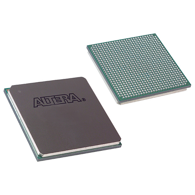
EP1AGX60DF780I6N
| Part Description |
Arria GX Field Programmable Gate Array (FPGA) IC 350 2528640 60100 780-BBGA |
|---|---|
| Quantity | 423 Available (as of October 7, 2026) |

| Product Category | Field Programmable Gate Array (FPGA) |
|---|---|
| Manufacturer | Intel |
| Manufacturing Status | Obsolete |
| Manufacturer Standard Lead Time | Contact Us |
| Datasheet |
Specifications & Environmental
| Device Package | 780-FBGA (29x29) | Grade | Industrial | Operating Temperature | -40°C – 100°C | ||
|---|---|---|---|---|---|---|---|
| Package / Case | 780-BBGA | Number of I/O | 350 | Voltage | 1.15 V - 1.25 V | ||
| Mounting Method | Surface Mount | RoHS Compliance | RoHS Compliant | REACH Compliance | REACH Unaffected | ||
| Moisture Sensitivity Level | 3 (168 Hours) | Number of LABs/CLBs | 3005 | Number of Logic Elements/Cells | 60100 | ||
| Number of Gates | N/A | ECCN | 3A001A7A | HTS Code | 8542.39.0001 | ||
| Qualification | N/A | Total RAM Bits | 2528640 |
Overview of EP1AGX60DF780I6N – Arria GX Field Programmable Gate Array (FPGA) IC 350 2528640 60100 780-BBGA
The EP1AGX60DF780I6N is an Arria GX family FPGA in a 780-ball BGA package designed for industrial applications requiring programmable logic with integrated high-speed serial capabilities. It pairs a 1.2‑V logic array architecture with approximately 2.53 Mbits of embedded memory and 60,100 logic elements to implement complex control, signal-processing, and protocol-handling functions.
With support for high-density I/O (350 pins), configurable transceiver functionality from the Arria GX family, and a wide supply and temperature range, this device is positioned for network, video, and high‑performance embedded processing designs that demand integration and flexibility.
Key Features
- Logic Capacity — 60,100 logic elements, suitable for substantial FPGA designs and complex custom logic integration.
- Embedded Memory — Approximately 2.53 Mbits of on-chip RAM for FIFOs, buffers, and temporary storage to support performance-critical datapaths.
- High‑Speed I/O & Transceivers — Family-level Arria GX transceiver architecture includes CDR-equipped SERDES with support for common serial protocols and high-speed serial links.
- I/O Count & Standards — 350 I/O pins with support for numerous single-ended and differential standards, enabling diverse interfacing options.
- Clocking & DSP — Arria GX family features multi‑PLL clocking (up to four enhanced PLLs) and high-speed DSP blocks for multiply-accumulate and FIR implementations.
- Memory Architecture — TriMatrix RAM architecture with multiple RAM block sizes for dual-port memory and FIFO implementations, with internal performance up to the family‑specified rates.
- Power & Supply — Operates from a supply range of 1.15 V to 1.25 V, enabling integration into standard 1.2 V FPGA power rails.
- Package & Mounting — 780‑BBGA package (supplier package: 780‑FBGA, 29×29) with surface-mount mounting for compact board integration.
- Industrial Grade & Temperature — Industrial grade device rated for operation from −40 °C to 100 °C.
- Compliance — RoHS‑compliant manufacturing status.
- IP & Configuration Support — Arria GX family supports Altera MegaCore IP and AMPP megafunctions and features for remote configuration and established protocol megafunctions.
Typical Applications
- Networking & Communications — Protocol offload, packet processing, and high-speed link interfacing where integrated transceivers and abundant I/O simplify board design.
- Video & Broadcast — SDI and other serial video protocol bridging and processing using the family’s SERDES and dedicated protocol support.
- High‑Performance Embedded Systems — DSP-heavy signal processing and algorithm acceleration leveraging on-chip DSP blocks and plentiful logic elements.
- Storage & Interface Controllers — Implement controllers and protocol bridges that require flexible I/O standards and on-chip memory for buffering.
Unique Advantages
- Integrated Serial Protocol Support: Family-level SERDES with CDR and protocol megafunction support reduces external chipset needs for high‑speed links.
- Balanced Logic and Memory: 60,100 logic elements coupled with approximately 2.53 Mbits of embedded RAM provide a balance suited to complex control and buffering tasks.
- Flexible Clocking and DSP: Enhanced PLLs and dedicated DSP blocks enable stable, high-performance signal processing and clock-domain management.
- Industrial Reliability: Rated for −40 °C to 100 °C operation and RoHS compliant, appropriate for industrial environments.
- High I/O Density: 350 I/O pins allow interfacing to a wide range of peripherals and high-speed external memory or transceiver connections.
- Compact Packaging: 780‑BBGA (29×29 FBGA supplier package) provides a high‑pin count solution in a compact surface‑mount form factor.
Why Choose EP1AGX60DF780I6N?
The EP1AGX60DF780I6N delivers a mid-to-high density Arria GX FPGA option that combines sizable logic capacity, multi-megabit embedded memory, and family-level high-speed transceiver capabilities in a single industrial-grade package. It is well suited for designs that require integrated serial protocol handling, significant on-chip processing, and flexible I/O options.
Designers benefit from the Arria GX family’s megafunction IP support, diverse clocking and DSP resources, and a package optimized for board-level density. The device is appropriate for network, video, and embedded signal-processing customers seeking a scalable, programmable platform with industrial operating range.
If you would like pricing, availability, or a formal quote for EP1AGX60DF780I6N, submit a request to receive a sales quotation or additional technical information.

























Date Founded: 1968
Headquarters: Santa Clara, California, USA
Employees: 130,000+
Revenue: $54.23 Billion
Certifications and Memberships: ISO9001:2015, ISO14001:2015, ISO17025:2017, ISO27001:2022, ISO45001:2018, ISO50001:2018


