
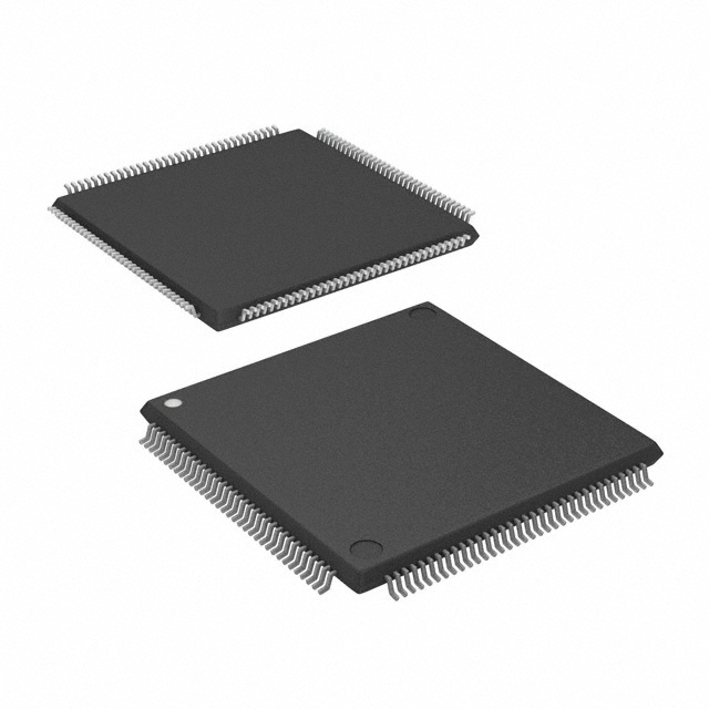
EP1K30TC144-3N
| Part Description |
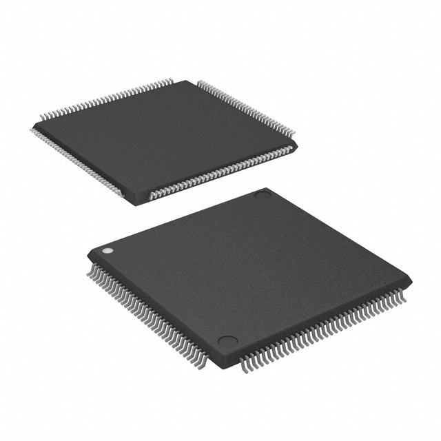
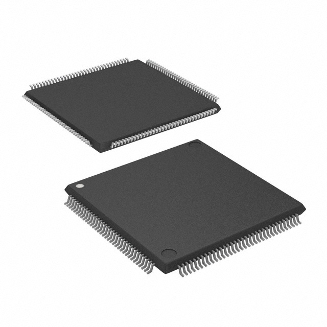
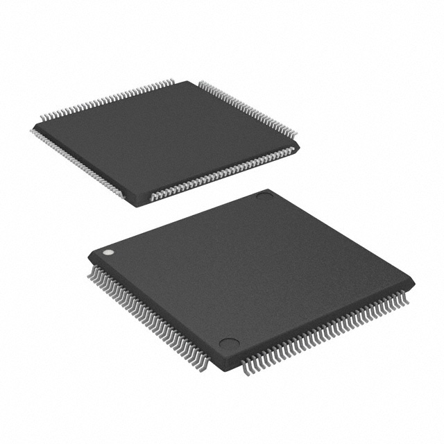
ACEX-1K® Field Programmable Gate Array (FPGA) IC 102 24576 1728 144-LQFP |
|---|---|
| Quantity | 691 Available (as of October 8, 2026) |
| Product Category | Field Programmable Gate Array (FPGA) |
|---|---|
| Manufacturer | Intel |
| Manufacturing Status | Obsolete |
| Manufacturer Standard Lead Time | Contact Us |
| Datasheet |
Specifications & Environmental
| Device Package | 144-TQFP (20x20) | Grade | Commercial | Operating Temperature | 0°C – 70°C | ||
|---|---|---|---|---|---|---|---|
| Package / Case | 144-LQFP | Number of I/O | 102 | Voltage | 2.375 V - 2.625 V | ||
| Mounting Method | Surface Mount | RoHS Compliance | Unknown | REACH Compliance | REACH Unaffected | ||
| Moisture Sensitivity Level | 3 (168 Hours) | Number of LABs/CLBs | 216 | Number of Logic Elements/Cells | 1728 | ||
| Number of Gates | 119000 | ECCN | 3A991D | HTS Code | 8542.39.0001 | ||
| Qualification | N/A | Total RAM Bits | 24576 |
Overview of EP1K30TC144-3N – ACEX-1K® Field Programmable Gate Array (FPGA) IC 102 24576 1728 144-LQFP
The EP1K30TC144-3N is an ACEX-1K series field programmable gate array (FPGA) optimized for cost-sensitive, high-integration applications. It pairs a logic array with an enhanced embedded array (EAB) architecture to implement both general logic and efficient on-chip memory functions.
This commercial-grade device is suited for system-on-a-programmable-chip (SOPC) tasks in communications and embedded control markets, offering a balance of logic capacity, embedded RAM, and flexible I/O for mixed-voltage systems.
Key Features
- Core Logic 1,728 logic elements provide programmable combinatorial and sequential logic capacity for custom functions and glue logic.
- On-Chip Memory Approximately 24,576 total RAM bits implemented via embedded array blocks (EABs) for efficient storage, small FIFOs, and dual-port memory configurations.
- I/O and Voltage Support 102 user I/O pins with MultiVolt capability described at the series level to interface with 2.5 V, 3.3 V, or 5.0 V devices; internal supply operates around 2.5 V with device supply specified at 2.375 V to 2.625 V.
- Performance Capacity Up to 119,000 maximum system gates (series table reference) for implementing sizeable logic functions and glue logic in a single device.
- Embedded Array Block (EAB) Features Enhanced EABs support dual-port operation and up to 16-bit width per block for flexible memory and specialized logic megafunctions (series-level capability).
- Configuration and Test In-circuit reconfigurability via external configuration devices or JTAG boundary-scan (IEEE 1149.1) for programming and test access (series-level feature).
- Package and Mounting Surface-mount 144-pin LQFP package; supplier device package listed as 144-TQFP (20×20), suitable for compact board layouts.
- Operating Range & Compliance Commercial grade with operating temperature 0 °C to 70 °C and RoHS-compliant manufacturing.
Typical Applications
- Communications Equipment Use the device’s logic and embedded memory to implement protocol glue logic, small packet buffers, and interface bridging in communications platforms.
- Embedded Control Implement control algorithms, peripheral aggregation, and custom I/O handling for industrial-style embedded systems operating within commercial temperature ranges.
- SOPC and Megafunction Integration Integrate multiple system functions—such as memory blocks, state machines, and interface logic—into a single FPGA to reduce BOM and simplify board-level design.
- Prototype and Low- to Mid-Volume Products Rapidly iterate designs that require reconfigurability and on-chip memory without committing to full ASIC development.
Unique Advantages
- High Integration Density: 1,728 logic elements and embedded RAM reduce external component count and PCB complexity.
- Flexible Memory Architecture: EABs with dual-port capability and up to 16-bit widths support efficient implementation of FIFOs, small data buffers, and megafunctions.
- Multi‑Voltage Interfacing: Series-level MultiVolt I/O support facilitates direct interfacing with 2.5 V, 3.3 V, and 5.0 V devices, easing mixed-voltage system design.
- Reconfigurability and Testability: In-circuit reconfiguration and JTAG boundary-scan support allow field updates and board-level test access without consuming user logic.
- Compact Packaging: 144-pin LQFP/TQFP packaging enables dense board layouts while maintaining a broad set of user I/Os.
- Regulatory and Environmental Compliance: RoHS-compliant construction supports environmental requirements for commercial products.
Why Choose EP1K30TC144-3N?
The EP1K30TC144-3N delivers a balanced combination of logic resources, embedded memory, and flexible I/O in a compact commercial-grade package. It is well suited for designers looking to consolidate multiple discrete functions into a single programmable device—reducing BOM and accelerating time to market while retaining the ability to reconfigure and iterate in the field.
This device is appropriate for engineering teams developing communications interfaces, embedded controllers, and SOPC-based systems that require moderate logic capacity, on-chip RAM, and multi-voltage interfacing within a 0 °C to 70 °C operating range.
Request a quote or submit an inquiry to get pricing, availability, and additional technical support information for the EP1K30TC144-3N.





















Date Founded: 1968
Headquarters: Santa Clara, California, USA
Employees: 130,000+
Revenue: $54.23 Billion
Certifications and Memberships: ISO9001:2015, ISO14001:2015, ISO17025:2017, ISO27001:2022, ISO45001:2018, ISO50001:2018


