
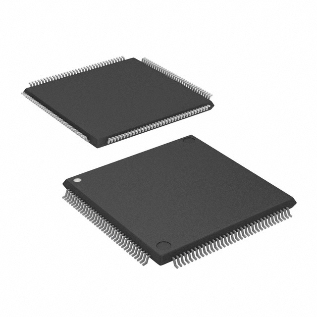
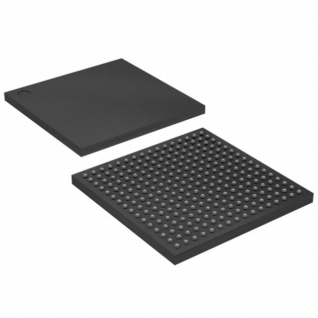
EP1K50FC256-1
| Part Description |
ACEX-1K® Field Programmable Gate Array (FPGA) IC 186 40960 2880 256-BGA |
|---|---|
| Quantity | 1,417 Available (as of June 15, 2026) |

| Product Category | Field Programmable Gate Array (FPGA) |
|---|---|
| Manufacturer | Intel |
| Manufacturing Status | Obsolete |
| Manufacturer Standard Lead Time | Contact Us |
| Datasheet |
Specifications & Environmental
| Device Package | 256-FBGA (17x17) | Grade | Commercial | Operating Temperature | 0°C – 70°C | ||
|---|---|---|---|---|---|---|---|
| Package / Case | 256-BGA | Number of I/O | 186 | Voltage | 2.375 V - 2.625 V | ||
| Mounting Method | Surface Mount | RoHS Compliance | RoHS non-compliant | REACH Compliance | REACH Unaffected | ||
| Moisture Sensitivity Level | 3 (168 Hours) | Number of LABs/CLBs | 360 | Number of Logic Elements/Cells | 2880 | ||
| Number of Gates | 199000 | ECCN | 3A991D | HTS Code | 8542.39.0001 | ||
| Qualification | N/A | Total RAM Bits | 40960 |
Overview of EP1K50FC256-1 – ACEX-1K® Field Programmable Gate Array (FPGA) IC 186 40960 2880 256-BGA
The EP1K50FC256-1 is an Intel ACEX-1K family FPGA delivering a balanced mix of logic, embedded memory, and I/O in a compact 256-FBGA surface-mount package. Targeted for cost-efficient system-on-a-programmable-chip integration, this device combines 2,880 logic elements with approximately 40,960 bits of embedded RAM to implement memory-intensive megafunctions and general logic.
Designed for commercial applications, the device operates from a 2.375 V to 2.625 V supply and across a 0 °C to 70 °C operating range, providing a practical, RoHS-compliant programmable logic option for communications, embedded control, and interface tasks.
Key Features
- Core Logic 2,880 logic elements (LEs) supporting up to 199,000 maximum system gates for implementing complex logic and control functions.
- Embedded Memory (EAB) Approximately 40,960 total RAM bits organized in embedded array blocks, enabling efficient on-chip storage for FIFOs, buffers, and megafunctions.
- I/O Capacity & Flexibility 186 user I/O pins with MultiVolt I/O capability (family feature) to interface with 2.5 V, 3.3 V, or 5.0 V devices and support mixed-voltage systems.
- Packaging 256-pin FineLine BGA (256-FBGA, 17×17) surface-mount package for high-pin-density designs and compact board real estate.
- Power and Temperature Operates with a 2.375–2.625 V supply range and specified for commercial-grade operation from 0 °C to 70 °C.
- Compliance and Testability Family-level features include JTAG boundary-scan (IEEE 1149.1) for in-system test and RoHS compliance for environmental requirements.
- System-Level Features Architecture provides dual-port embedded array capability and dedicated routing resources suitable for implementing megafunctions and high-fan-in logic (family-level features).
Typical Applications
- Communications and Networking Packet processing, protocol bridging, and hardware acceleration where embedded memory and flexible I/O reduce external component count.
- Embedded Systems On-board control logic, custom peripherals, and state machines benefiting from reprogrammability and integrated RAM.
- Interface and Glue Logic Voltage-domain bridging and timing adaptation between modules using the device’s high I/O count and MultiVolt capability.
- Memory and Buffering Functions FIFOs, small buffers, and lookup tables implemented using the on-chip EABs to reduce PCB BOM and latency.
Unique Advantages
- Balanced Logic-to-Memory Ratio: 2,880 logic elements paired with ~40,960 bits of embedded RAM supports integrated megafunctions without immediate external memory.
- High I/O Density in a Compact Package: 186 I/O pins in a 256-FBGA (17×17) footprint enables complex interfacing while conserving PCB area.
- Commercial-Grade Reliability: Specified operating range of 0 °C to 70 °C and RoHS compliance align with standard commercial product requirements.
- Flexible Voltage Integration: MultiVolt I/O capabilities facilitate mixed-voltage system integration and simplify board-level power domain management.
- Test and Reconfiguration Support: JTAG boundary-scan support and in-circuit reconfigurability (family features) help streamline production test and field updates.
Why Choose EP1K50FC256-1?
The EP1K50FC256-1 offers a pragmatic combination of logic resources, embedded memory, and dense I/O in a compact 256-FBGA package, making it well suited for designers who need on-chip buffering, interface logic, and reprogrammable functionality without a large form factor. Its family-proven features for embedded arrays, flexible I/O voltages, and boundary-scan testability provide integration and manufacturing advantages for commercial applications.
This device fits projects that require mid-range programmable logic capacity with on-chip RAM, such as communications peripherals, embedded control circuits, and interface bridging—delivering a scalable, RoHS-compliant platform with clear electrical and thermal operating bounds.
Request a quote or submit an inquiry to get pricing and availability for the EP1K50FC256-1.


Date Founded: 1968
Headquarters: Santa Clara, California, USA
Employees: 130,000+
Revenue: $54.23 Billion
Certifications and Memberships: ISO9001:2015, ISO14001:2015, ISO17025:2017, ISO27001:2022, ISO45001:2018, ISO50001:2018


