
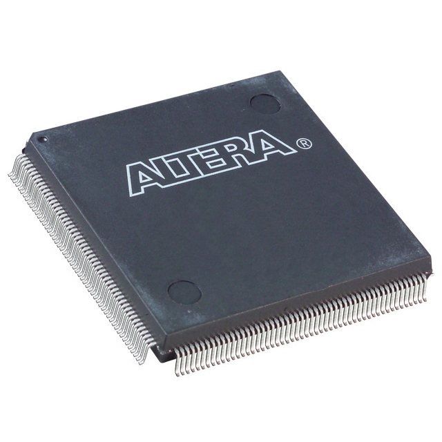
EP1K50QC208-3AA
| Part Description |
ACEX-1K® Field Programmable Gate Array (FPGA) IC 147 40960 2880 208-BFQFP |
|---|---|
| Quantity | 978 Available (as of June 14, 2026) |
| Product Category | Field Programmable Gate Array (FPGA) |
|---|---|
| Manufacturer | Intel |
| Manufacturing Status | Obsolete |
| Manufacturer Standard Lead Time | Contact Us |
| Datasheet |
Specifications & Environmental
| Device Package | 208-PQFP (28x28) | Grade | Commercial | Operating Temperature | 0°C – 70°C | ||
|---|---|---|---|---|---|---|---|
| Package / Case | 208-BFQFP | Number of I/O | 147 | Voltage | 2.375 V - 2.625 V | ||
| Mounting Method | Surface Mount | RoHS Compliance | Unknown | REACH Compliance | REACH Unknown | ||
| Moisture Sensitivity Level | 3 (168 Hours) | Number of LABs/CLBs | 360 | Number of Logic Elements/Cells | 2880 | ||
| Number of Gates | 199000 | ECCN | OBSOLETE | HTS Code | 0000.00.0000 | ||
| Qualification | N/A | Total RAM Bits | 40960 |
Overview of EP1K50QC208-3AA – ACEX-1K FPGA, 2,880 logic elements, 208-BFQFP
The EP1K50QC208-3AA is an ACEX-1K family Field Programmable Gate Array (FPGA) designed for mid-density, cost-sensitive system integration. The device combines 2,880 logic elements with approximately 40,960 bits of embedded RAM to implement on-chip memory and specialized logic functions within a single programmable device.
Targeted at system-on-a-programmable-chip (SOPC) and communications-oriented designs, this commercial-grade FPGA delivers flexible I/O, in-circuit reconfigurability, and packaging options suitable for surface-mount assembly.
Key Features
- Logic Capacity — 2,880 logic elements providing up to 199,000 system gates for mid-range logic integration and glue-logic consolidation.
- On‑Chip Memory — Approximately 40,960 bits of embedded RAM (EABs) with dual-port capability for efficient implementation of buffers, FIFOs, and small data stores.
- I/O and Voltage Support — 147 user I/O pins with MultiVolt I/O capability described by the ACEX-1K family; device-level supply range is 2.375 V to 2.625 V and the device operates with a 2.5‑V internal supply.
- Clocking and Performance — Built-in low-skew clock distribution and options such as ClockLock and ClockBoost (family features) to reduce clock delay and skew in synchronous designs.
- Configuration and Test — In-circuit reconfigurability (ICR) via external configuration devices, intelligent controllers, or the JTAG port; includes IEEE 1149.1 boundary-scan test support.
- Package and Mounting — 208-BFQFP package case; supplier device package listed as 208‑PQFP (28×28); surface-mount mounting type for compact PCB layouts.
- Environmental and Reliability — Commercial grade with an operating temperature range of 0 °C to 70 °C and RoHS-compliant materials.
Typical Applications
- Communications Interfaces — Implement protocol bridging, packet buffering, and timing-critical data paths using embedded RAM and dedicated carry/cascade resources.
- SOPC and Embedded Control — Integrate custom logic, peripheral glue, and small memories to consolidate multiple discrete components into a single programmable device.
- Peripheral and Bus Glue Logic — Use the device’s moderate logic density and flexible I/O to interface between controllers, memory, and external peripherals.
- Prototyping and Low‑Volume Production — Ideal for designs that require reconfigurability during development and modest production volumes in commercial applications.
Unique Advantages
- Balanced Logic and Memory: The combination of 2,880 logic elements and ~40,960 bits of embedded RAM enables both control logic and local data storage without external SRAM for many mid-range designs.
- Flexible I/O and Voltage Compatibility: MultiVolt I/O family features and 147 user I/Os simplify interfacing to a variety of peripheral voltage domains while using a standard 2.5‑V internal supply.
- In-Circuit Reconfigurability: Support for ICR and JTAG boundary-scan streamlines iterative development and field updates without board-level hardware changes.
- Surface-Mount Packaging: 208-pin PQFP/BFQFP packaging supports compact PCB layouts and established assembly processes.
- Testability and Standards Support: Built-in JTAG (IEEE 1149.1) boundary-scan and family-level compliance notes (e.g., PCI compatibility options in the family datasheet) aid verification and integration in standard systems.
- RoHS Compliant: Materials and manufacturing meet RoHS requirements for current commercial designs.
Why Choose EP1K50QC208-3AA?
The EP1K50QC208-3AA positions itself as a practical, reconfigurable solution for developers needing moderate logic capacity with substantial on-chip RAM. Its mix of 2,880 logic elements, dual-port embedded memory, and flexible I/O makes it well suited for communications interfaces, SOPC implementations, and peripheral bridging where board space and component count are priorities.
For engineering teams and procurement groups focused on commercial applications, this ACEX-1K device delivers a predictable temperature and supply envelope, surface-mount packaging for compact designs, and features that support in-system configuration and testability—helping to shorten development cycles and simplify integration.
Request a quote or submit a procurement inquiry to begin sourcing EP1K50QC208-3AA for your next design.


Date Founded: 1968
Headquarters: Santa Clara, California, USA
Employees: 130,000+
Revenue: $54.23 Billion
Certifications and Memberships: ISO9001:2015, ISO14001:2015, ISO17025:2017, ISO27001:2022, ISO45001:2018, ISO50001:2018


