
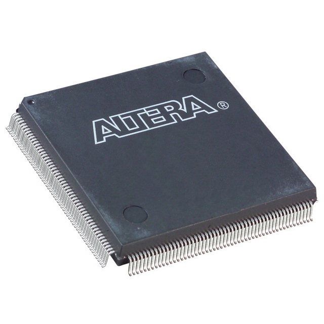
EP1K50QC208-2N
| Part Description |
ACEX-1K® Field Programmable Gate Array (FPGA) IC 147 40960 2880 208-BFQFP |
|---|---|
| Quantity | 400 Available (as of June 15, 2026) |

| Product Category | Field Programmable Gate Array (FPGA) |
|---|---|
| Manufacturer | Intel |
| Manufacturing Status | Obsolete |
| Manufacturer Standard Lead Time | Contact Us |
| Datasheet |
Specifications & Environmental
| Device Package | 208-PQFP (28x28) | Grade | Commercial | Operating Temperature | 0°C – 70°C | ||
|---|---|---|---|---|---|---|---|
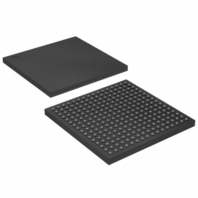
| Package / Case | 208-BFQFP | Number of I/O | 147 | Voltage | 2.375 V - 2.625 V | ||
| Mounting Method | Surface Mount | RoHS Compliance | Unknown | REACH Compliance | REACH Unaffected | ||
| Moisture Sensitivity Level | 3 (168 Hours) | Number of LABs/CLBs | 360 | Number of Logic Elements/Cells | 2880 | ||
| Number of Gates | 199000 | ECCN | 3A991D | HTS Code | 8542.39.0001 | ||
| Qualification | N/A | Total RAM Bits | 40960 |
Overview of EP1K50QC208-2N – ACEX-1K® Field Programmable Gate Array (FPGA) IC 147 40960 2880 208-BFQFP
The EP1K50QC208-2N is an ACEX-1K family FPGA from Intel, offering a programmable logic fabric with embedded memory and flexible I/O for commercial applications. Built for system-on-a-programmable-chip (SOPC) integration, it combines mid-range logic density with dedicated memory blocks and configurable I/O to address communications, peripheral interfacing, and general-purpose logic acceleration.
Key architectural elements include approximately 2,880 logic elements, 40,960 bits of embedded RAM, and support for multi-voltage I/O. The device ships in a 208-BFQFP surface-mount package and is specified for commercial operation from 0 °C to 70 °C.
Key Features
- Logic Capacity — Approximately 2,880 logic elements and up to 199,000 system gates provide mid-range programmable logic for glue logic, state machines, and custom datapaths.
- Embedded Memory (EABs) — Series-level architecture includes embedded array blocks (EABs) enabling a total of 40,960 RAM bits for FIFOs, buffers, and small on-chip data storage.
- I/O Density & Flexibility — 147 user I/O pins with MultiVolt capability allow interfacing with 2.5-V, 3.3-V, or 5.0-V devices (series feature); individual pin options include programmable slew rate and open-drain modes.
- Supply & Power — Device supply range is specified as 2.375 V to 2.625 V; the ACEX-1K family operates with a 2.5-V internal supply voltage (series characteristic).
- Reconfiguration & Test — Supports in-circuit reconfigurability (ICR) and includes JTAG boundary-scan test (IEEE Std. 1149.1) circuitry for board-level testability without consuming user logic.
- Package & Mounting — 208-BFQFP (supplier package 208-PQFP, 28×28) in a surface-mount form factor suitable for compact PCB designs.
- Commercial Grade & Environmental — Rated for commercial temperature range 0 °C to 70 °C and RoHS compliant.
Typical Applications
- Communications Interfaces — Use the device’s logic density and embedded RAM for protocol bridging, packet buffering, and control-plane logic in communications equipment.
- SOPC Integration — Integrate custom accelerators, glue logic, and peripheral controllers into a single programmable device to reduce board-level BOM.
- Peripheral & Bus Glue — Implement bus translators, interface timing adjustments, and device-level controllers using the device’s flexible I/O and reconfigurability.
- Memory Buffering & FIFO — Leverage on-chip embedded RAM blocks for small FIFO and buffer implementations in data path designs.
Unique Advantages
- Balanced Logic and Memory — Combining ~2,880 logic elements with 40,960 bits of embedded RAM delivers a balanced platform for control logic plus local buffering.
- Multi-Voltage I/O Support — MultiVolt I/O enables direct interfacing to a variety of external devices without additional level shifters, simplifying board design.
- Reconfigurable In-Circuit — In-circuit reconfigurability and JTAG support simplify field updates and board-level test integration.
- Compact Surface-Mount Package — The 208-BFQFP package provides a space-efficient footprint for compact commercial designs.
- Commercial Temperature & RoHS Compliance — Specified for 0 °C to 70 °C operation and RoHS compliant for regulatory and manufacturing consistency.
Why Choose EP1K50QC208-2N?
The EP1K50QC208-2N positions itself as a practical, mid-density FPGA for commercial applications that require a mix of programmable logic, embedded RAM, and flexible I/O in a compact package. Its combination of roughly 2,880 logic elements, 40,960 bits of embedded memory, and 147 I/O pins makes it suitable for SOPC integration, communication interfaces, and board-level glue logic where reconfigurability and in-circuit updates are valuable.
Designed and supplied by Intel, the device benefits from a family-level architecture that includes features such as MultiVolt I/O, JTAG boundary-scan, and dedicated memory blocks — helping teams reduce BOM, accelerate development, and maintain field-updatable designs for commercial product lines.
Request a quote or submit an inquiry to receive pricing, availability, and technical support information for the EP1K50QC208-2N.


Date Founded: 1968
Headquarters: Santa Clara, California, USA
Employees: 130,000+
Revenue: $54.23 Billion
Certifications and Memberships: ISO9001:2015, ISO14001:2015, ISO17025:2017, ISO27001:2022, ISO45001:2018, ISO50001:2018


