
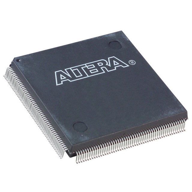
EP1K50QC208-3
| Part Description |
ACEX-1K® Field Programmable Gate Array (FPGA) IC 147 40960 2880 208-BFQFP |
|---|---|
| Quantity | 1,093 Available (as of June 14, 2026) |

| Product Category | Field Programmable Gate Array (FPGA) |
|---|---|
| Manufacturer | Intel |
| Manufacturing Status | Obsolete |
| Manufacturer Standard Lead Time | Contact Us |
| Datasheet |
Specifications & Environmental
| Device Package | 208-PQFP (28x28) | Grade | Commercial | Operating Temperature | 0°C – 70°C | ||
|---|---|---|---|---|---|---|---|
| Package / Case | 208-BFQFP | Number of I/O | 147 | Voltage | 2.375 V - 2.625 V | ||
| Mounting Method | Surface Mount | RoHS Compliance | RoHS non-compliant | REACH Compliance | REACH Unaffected | ||
| Moisture Sensitivity Level | 3 (168 Hours) | Number of LABs/CLBs | 360 | Number of Logic Elements/Cells | 2880 | ||
| Number of Gates | 199000 | ECCN | 3A991D | HTS Code | 8542.39.0001 | ||
| Qualification | N/A | Total RAM Bits | 40960 |
Overview of EP1K50QC208-3 – ACEX-1K Field Programmable Gate Array (FPGA) IC, 208-BFQFP
The EP1K50QC208-3 is an ACEX-1K family FPGA delivering a balance of logic capacity, embedded memory, and flexible I/O in a 208-pin BFQFP package. Built for cost-efficient system integration, the device combines a logic array and embedded array blocks (EABs) to implement memory and specialized megafunctions for communications and general-purpose embedded designs.
With 2,880 logic elements, approximately 40,960 bits of embedded RAM, and 147 user I/O pins, this commercial-grade device targets mid-density FPGA applications that require reconfigurability, multi-voltage I/O capability, and compact surface-mount packaging.
Key Features
- Logic Capacity 2,880 logic elements (LEs) and up to 199,000 maximum system gates provide mid-density programmable logic suitable for control, glue logic, and moderate-complexity digital functions.
- Embedded Memory (EABs) Ten embedded array blocks (EABs) totaling approximately 40,960 bits of RAM; EABs support dual-port operation and up to 16-bit width per block for efficient megafunction implementation.
- I/O and Voltage 147 user I/O pins with MultiVolt I/O capability described in the ACEX-1K family documentation; device operates with an internal supply in the 2.375 V to 2.625 V range as specified.
- Package & Mounting 208-BFQFP package (supplier device package: 208-PQFP, 28×28); surface-mount mounting type suited for compact PCB layouts.
- Configuration & Test Supports in-circuit reconfigurability via external configuration devices, intelligent controller, or JTAG; built-in JTAG boundary-scan test circuitry compliant with IEEE Std. 1149.1-1990.
- Clocking & Interconnect On-chip low-skew clock distribution, options for ClockLock and ClockBoost, dedicated carry and cascade chains, and FastTrack interconnect architecture for predictable routing delays.
- Operating Conditions Commercial grade with an operating temperature range of 0 °C to 70 °C and RoHS compliance.
Typical Applications
- Communications Equipment Implements protocol glue logic, buffering and mid-density packet processing where reconfigurability and embedded RAM are required.
- System-on-a-Programmable-Chip (SOPC) Combines logic and EAB-based memory to integrate controllers, peripheral interfaces, and custom glue logic into a single programmable device.
- Embedded Control and Interface Handles sensor interfacing, motor-control glue logic, and user-interface control with flexible I/O and programmable logic resources.
- Prototyping and Evaluation Well-suited for board- and system-level prototyping where moderate logic density and reconfigurability speed design iterations.
Unique Advantages
- Balanced integration: Combines 2,880 logic elements with ten EABs (~40,960 bits) to reduce external memory and simplify BOM for mid-range designs.
- Flexible I/O signaling: MultiVolt I/O capability allows interface with a range of external devices while the device core runs within the specified 2.375 V–2.625 V supply window.
- Built-in test and configuration: JTAG boundary-scan and in-circuit reconfigurability streamline board bring-up and field updates without consuming user logic.
- Deterministic routing and arithmetic support: FastTrack interconnect plus dedicated carry and cascade chains yield predictable timing for adders, counters, and high-fan-in logic.
- Compact surface-mount package: 208-pin BFQFP (28×28 PQFP footprint) enables dense PCB layouts while providing ample I/O for a wide variety of applications.
Why Choose EP1K50QC208-3?
The EP1K50QC208-3 positions itself as a practical mid-density FPGA choice when you need a mix of programmable logic, embedded memory, and flexible I/O in a compact, surface-mount package. Its combination of 2,880 logic elements, ten EABs (approximately 40,960 bits), and 147 I/O pins supports system-level integration tasks that reduce external components and shorten development cycles.
Designed for commercial applications, the device provides in-circuit reconfigurability, industry-standard boundary-scan test, and predictable routing and clocking features that help engineers implement and validate designs efficiently. It is suited to teams targeting communications, embedded control, and SOPC-style integration where mid-range capacity and reconfigurability deliver long-term design flexibility.
Request a quote or submit a procurement inquiry to obtain pricing, availability, and lead-time information for the EP1K50QC208-3.


Date Founded: 1968
Headquarters: Santa Clara, California, USA
Employees: 130,000+
Revenue: $54.23 Billion
Certifications and Memberships: ISO9001:2015, ISO14001:2015, ISO17025:2017, ISO27001:2022, ISO45001:2018, ISO50001:2018


