
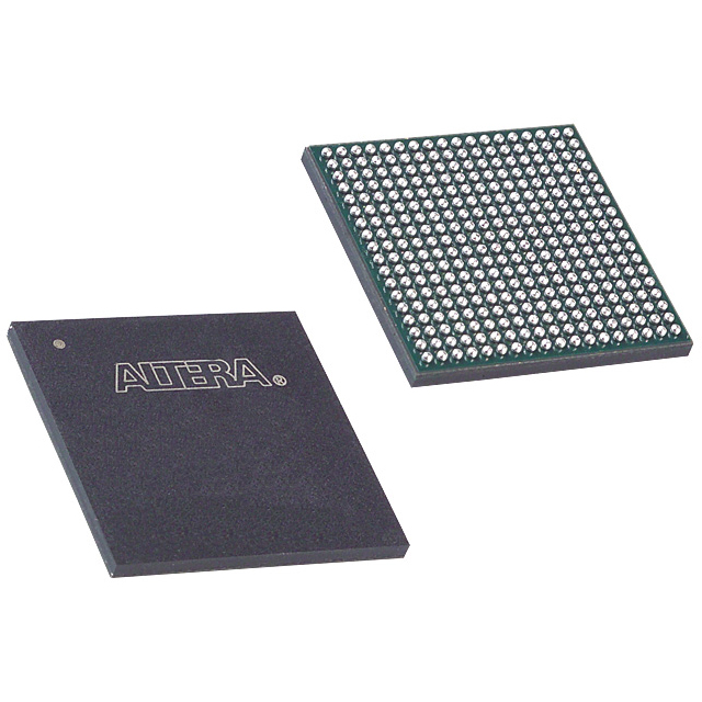
EP20K100FC324-1V
| Part Description |
APEX-20K® Field Programmable Gate Array (FPGA) IC 252 53248 4160 324-BGA |
|---|---|
| Quantity | 495 Available (as of June 17, 2026) |

| Product Category | Field Programmable Gate Array (FPGA) |
|---|---|
| Manufacturer | Intel |
| Manufacturing Status | Obsolete |
| Manufacturer Standard Lead Time | Contact Us |
| Datasheet |
Specifications & Environmental
| Device Package | 324-FBGA (19x19) | Grade | Commercial | Operating Temperature | 0°C – 85°C | ||
|---|---|---|---|---|---|---|---|
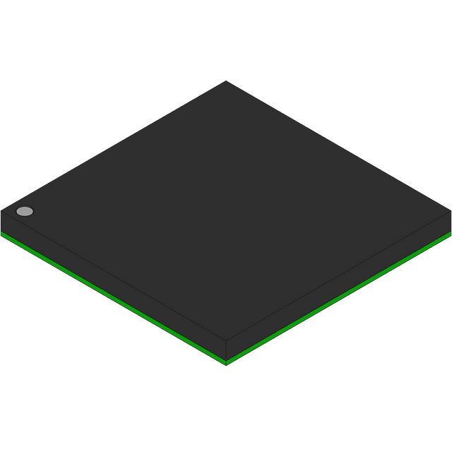
| Package / Case | 324-BGA | Number of I/O | 252 | Voltage | 2.375 V - 2.625 V | ||
| Mounting Method | Surface Mount | RoHS Compliance | RoHS non-compliant | REACH Compliance | REACH Unaffected | ||
| Moisture Sensitivity Level | 3 (168 Hours) | Number of LABs/CLBs | 416 | Number of Logic Elements/Cells | 4160 | ||
| Number of Gates | 263000 | ECCN | 3A991D | HTS Code | 8542.39.0001 | ||
| Qualification | N/A | Total RAM Bits | 53248 |
Overview of EP20K100FC324-1V – APEX-20K Field Programmable Gate Array, 324‑BGA
The EP20K100FC324-1V is an APEX-20K family FPGA in a 324‑ball FBGA (19×19) surface‑mount package. It integrates 4,160 logic elements and approximately 53,248 bits of embedded memory to support control, interface and mid‑density logic integration in commercial‑grade designs.
Designed for system integration and flexible I/O, this device targets applications needing sizeable on‑chip memory, multiple I/O interfaces and configurable clock management while operating within a 2.375 V to 2.625 V supply window and a 0 °C to 85 °C commercial temperature range.
Key Features
- Logic Capacity — 4,160 logic elements (LEs) and approximately 263,000 system gates provide mid‑range programmable logic resources for glue‑logic, protocol bridging and control functions.
- Embedded Memory — Approximately 53,248 bits of on‑chip RAM arranged in Embedded System Blocks (ESBs) for implementing FIFOs, dual‑port RAM or content‑addressable memory.
- I/O Density & Flexibility — 252 user I/O pins with MultiVolt I/O interface support, enabling direct interfacing to multiple voltage domains used in mixed‑signal systems.
- Clocking & Timing — Family features include flexible clock management with up to four phase‑locked loops (PLLs), a built‑in low‑skew clock tree and support for multiple global clock signals for synchronous system design.
- Power — Specified operating supply range of 2.375 V to 2.625 V; device family supports low‑power operation and power‑saving modes in ESBs.
- Package & Mounting — 324‑BGA (324‑FBGA, 19×19) surface‑mount package for compact board integration and high I/O count.
- Commercial Grade — Operating temperature range 0 °C to 85 °C and RoHS compliance for standard commercial applications.
Typical Applications
- Protocol Bridging and Interface Control — Use the device’s 252 I/O pins and MultiVolt I/O support to bridge logic levels and implement custom interface logic between subsystems.
- Embedded Memory Functions — Implement FIFO buffering, packet buffering or small dual‑port RAM structures using the on‑chip ESB memory.
- Control and Glue Logic — Deploy the 4,160 logic elements for timing, control sequencing, and peripheral management tasks in systems where integration reduces PCB BOM.
- Custom I/O and Timing Solutions — Leverage the device’s PLLs and clock tree to generate and distribute multiple clock domains for synchronized I/O and peripheral timing requirements.
Unique Advantages
- Balanced Logic and Memory — A combination of 4,160 logic elements and approximately 53 kbits of embedded RAM enables both compute and buffering on a single device, reducing the need for discrete components.
- High I/O Count in a Compact Package — 252 user I/Os in a 324‑ball FBGA (19×19) allows dense connectivity while preserving board area.
- Flexible Clock Management — Up to four PLLs and a low‑skew clock distribution framework simplify multi‑domain clocking and timing closure in complex designs.
- MultiVolt I/O Support — I/O interface flexibility eases integration with 2.5 V, 3.3 V and 5.0 V systems commonly found in mixed‑voltage designs.
- Commercial Temperature Suitability — Rated for 0 °C to 85 °C for a wide range of commercial electronics applications.
Why Choose EP20K100FC324-1V?
The EP20K100FC324-1V positions itself as a mid‑density FPGA option within the APEX‑20K family, combining 4,160 logic elements, substantial on‑chip RAM, and 252 I/O pins in a 324‑ball FBGA package. This mix of resources and package density is well suited to designers who need to consolidate interface logic, buffering and timing control into a single programmable device while operating within a standard commercial environment.
For teams focused on reducing board complexity and integrating multiple custom functions without exceeding commercial temperature and supply constraints, this device offers measurable integration benefits and predictable supply‑voltage and packaging characteristics backed by family‑level architecture features such as embedded system blocks and flexible PLL‑based clocking.
Request a quote or submit your procurement inquiry to receive pricing and availability for the EP20K100FC324-1V.


Date Founded: 1968
Headquarters: Santa Clara, California, USA
Employees: 130,000+
Revenue: $54.23 Billion
Certifications and Memberships: ISO9001:2015, ISO14001:2015, ISO17025:2017, ISO27001:2022, ISO45001:2018, ISO50001:2018


