
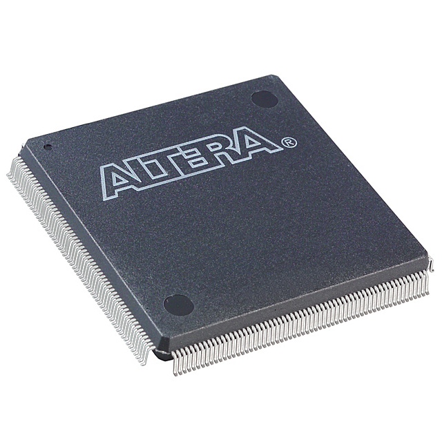
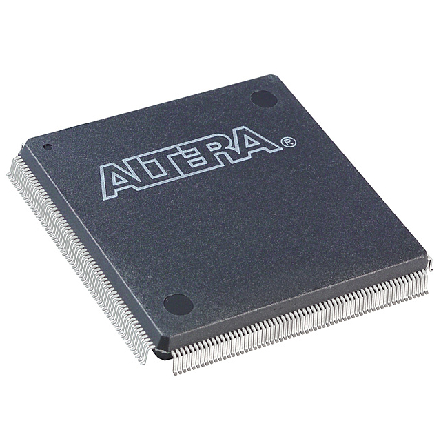
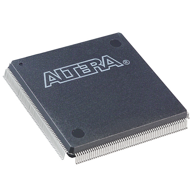
EP20K200EQC240-2N
| Part Description |
APEX-20KE® Field Programmable Gate Array (FPGA) IC 168 106496 8320 240-BFQFP |
|---|---|
| Quantity | 790 Available (as of October 8, 2026) |

| Product Category | Field Programmable Gate Array (FPGA) |
|---|---|
| Manufacturer | Intel |
| Manufacturing Status | Obsolete |
| Manufacturer Standard Lead Time | Contact Us |
| Datasheet |
Specifications & Environmental
| Device Package | 240-PQFP (32x32) | Grade | Commercial | Operating Temperature | 0°C – 85°C | ||
|---|---|---|---|---|---|---|---|
| Package / Case | 240-BFQFP | Number of I/O | 168 | Voltage | 1.71 V - 1.89 V | ||
| Mounting Method | Surface Mount | RoHS Compliance | Unknown | REACH Compliance | REACH Unaffected | ||
| Moisture Sensitivity Level | 3 (168 Hours) | Number of LABs/CLBs | 832 | Number of Logic Elements/Cells | 8320 | ||
| Number of Gates | 526000 | ECCN | 3A991D | HTS Code | 8542.39.0001 | ||
| Qualification | N/A | Total RAM Bits | 106496 |
Overview of EP20K200EQC240-2N – APEX-20KE® Field Programmable Gate Array (FPGA) IC 168 106496 8320 240-BFQFP
The EP20K200EQC240-2N is a commercial-grade FPGA from Intel's APEX 20K family, offering a MultiCore architecture that integrates look-up table (LUT) logic and embedded memory blocks (ESBs) for system-level programmability. With 8,320 logic elements and approximately 0.106 Mbits of embedded memory, this device targets mid-density designs that require on-chip RAM, flexible I/O, and integrated clock management.
Designed for system integration, the device supports a wide range of I/O standards and includes features for low-power operation and advanced clock control, making it suitable for applications needing memory buffering, protocol bridging, and custom logic implementation within a 240-pin BFQFP surface-mount package.
Key Features
- Core Architecture MultiCore architecture with LUT-based logic and embedded system blocks (ESBs) for register-intensive and memory functions.
- Logic Density 8,320 logic elements and a maximum of 526,000 system gates provide the capacity for mid-density programmable designs.
- Embedded Memory Approximately 0.106 Mbits of on-chip RAM (106,496 bits) usable without reducing available logic resources.
- I/O and Interface Support 168 user I/O pins with MultiVolt I/O interface support to interoperate with 1.8 V, 2.5 V, 3.3 V, and 5.0 V device levels; supports advanced I/O standards and high-speed memory interfaces.
- Clock Management Flexible clock circuitry including up to four PLLs, a low-skew clock tree, and multiple global clock signals for complex timing domains.
- Power and Voltage Internal supply range specified at 1.71 V to 1.89 V and designed for low-power operation; ESBs offer programmable power-saving modes.
- Package and Mounting Surface-mount 240-BFQFP package (240-PQFP, 32×32) suitable for compact board-level integration.
- Operating Range & Compliance Commercial grade with an operating temperature of 0 °C to 85 °C and RoHS compliance.
Typical Applications
- Embedded System Integration Implement SOPC-style system blocks and combine custom logic with on-chip memory for compact, integrated designs.
- High-Speed Interface Bridging Use flexible MultiVolt I/O and support for high-speed memory interfaces to bridge between different bus standards and external memories.
- Data Buffering and Packet Processing Leverage ESBs and on-chip RAM for FIFO buffers, dual-port RAM, and other buffering tasks in data-path applications.
- Prototyping and Custom Logic Deploy 8,320 logic elements and extensive clock-management to prototype and validate custom digital logic and control systems.
Unique Advantages
- Highly integrated logic and memory: Combine 8,320 logic elements with approximately 0.106 Mbits of embedded RAM to implement complex designs on a single device.
- Flexible I/O compatibility: MultiVolt I/O support and a broad set of supported I/O standards enable direct interfacing with many external components and memory types.
- Deterministic clocking: Multiple PLLs, a low-skew clock tree, and several global clocks simplify timing across multiple domains and reduce clock skew challenges.
- Compact package with high pin count: 240-pin BFQFP surface-mount package provides a high pin count and compact footprint for space-constrained boards.
- Commercial-grade reliability and compliance: Rated for 0 °C to 85 °C operation and RoHS compliant for standard commercial applications.
Why Choose EP20K200EQC240-2N?
The EP20K200EQC240-2N delivers a balanced combination of mid-level logic capacity, embedded memory, and flexible I/O in a commercial-grade FPGA package. As part of the APEX 20K family from Intel, it brings established architecture elements—LUT logic, ESBs, and advanced clocking—that simplify system integration and on-chip memory usage for buffering and control functions.
This device is well-suited for engineers and teams implementing embedded systems, interface bridging, and custom digital logic where predictable clocking, MultiVolt I/O, and a compact 240-pin BFQFP footprint are required. Its resource mix and family-level feature set support scalable designs and straightforward migration within the APEX 20K product line.
Request a quote or submit an inquiry to receive pricing and availability information for the EP20K200EQC240-2N.


























Date Founded: 1968
Headquarters: Santa Clara, California, USA
Employees: 130,000+
Revenue: $54.23 Billion
Certifications and Memberships: ISO9001:2015, ISO14001:2015, ISO17025:2017, ISO27001:2022, ISO45001:2018, ISO50001:2018


