LFE2M100SE-7FN900C
| Part Description |
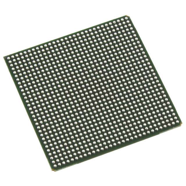
ECP2M Field Programmable Gate Array (FPGA) IC 416 5435392 95000 900-BBGA |
|---|---|
| Quantity | 318 Available (as of June 15, 2026) |

| Product Category | Field Programmable Gate Array (FPGA) |
|---|---|
| Manufacturer | Lattice Semiconductor Corporation |
| Manufacturing Status | Active |
| Manufacturer Standard Lead Time | 20 Weeks |
| Datasheet |
Specifications & Environmental
| Device Package | 900-FPBGA (31x31) | Grade | Commercial | Operating Temperature | 0°C – 85°C | ||
|---|---|---|---|---|---|---|---|
| Package / Case | 900-BBGA | Number of I/O | 416 | Voltage | 1.14 V - 1.26 V | ||
| Mounting Method | Surface Mount | RoHS Compliance | ROHS3 Compliant | REACH Compliance | REACH Unaffected | ||
| Moisture Sensitivity Level | 3 (168 Hours) | Number of LABs/CLBs | 11875 | Number of Logic Elements/Cells | 95000 | ||
| Number of Gates | N/A | ECCN | 3A991D | HTS Code | 8542.39.0001 | ||
| Qualification | N/A | Total RAM Bits | 5435392 |
Overview of LFE2M100SE-7FN900C – ECP2M Field Programmable Gate Array (FPGA), 95,000 LEs, 416 I/O, 900-BBGA
The LFE2M100SE-7FN900C is an ECP2M family Field Programmable Gate Array (FPGA) IC offered in a 900-BBGA package. It provides a high logic element count together with substantial embedded memory and a large I/O complement, packaged for surface-mount applications.
Designed for commercial-grade electronic designs, this device delivers programmable logic capacity, on-chip RAM and a broad I/O set while operating over a 1.14 V to 1.26 V supply range and a 0 °C to 85 °C temperature range.
Key Features
- Logic Capacity — 95,000 logic elements provide extensive programmable logic resources for complex designs and high-density implementations.
- Embedded Memory — Approximately 5.44 Mbits of on-chip RAM (5,435,392 bits) to support buffering, state storage and data processing functions.
- I/O — 416 general-purpose I/O pins to support wide connectivity and multiple peripheral interfaces.
- Power — Operates from a 1.14 V to 1.26 V supply range for core power compatibility in modern system architectures.
- Package and Mounting — 900-BBGA package case with supplier device package 900-FPBGA (31×31) designed for surface-mount assembly.
- Grade and Temperature — Commercial-grade device specified for operation from 0 °C to 85 °C.
- Environmental Compliance — RoHS compliant.
Unique Advantages
- High-density programmable logic: 95,000 logic elements enable integration of complex functions on a single device, reducing external component count.
- Substantial on-chip memory: Approximately 5.44 Mbits of embedded RAM supports local buffering and state storage, minimizing external memory dependency.
- Extensive I/O capability: 416 I/O pins allow flexible interfacing to sensors, peripherals and system buses without additional multiplexing hardware.
- Compact surface-mount package: 900-BBGA (900-FPBGA, 31×31) offers a high-pin-count footprint in a compact form factor for space-constrained PCBs.
- Commercial-grade operating range: Specified for 0 °C to 85 °C operation, suitable for mainstream consumer and industrial-adjacent applications.
- RoHS compliant: Supports regulatory requirements for lead-free assemblies.
Why Choose LFE2M100SE-7FN900C?
The LFE2M100SE-7FN900C positions itself as a high-capacity, commercial-grade FPGA option for designers who need substantial logic density, embedded memory and a broad I/O set in a compact BGA package. Its combination of 95,000 logic elements, approximately 5.44 Mbits of on-chip RAM and 416 I/O pins makes it suitable for systems that consolidate multiple functions into a single programmable device.
Choose this device when you require a balance of integration and configurability with RoHS compliance and standard commercial operating conditions. The package and power characteristics support modern surface-mount assembly and system-level power architectures.
Request a quote or submit an inquiry to receive pricing and availability for the LFE2M100SE-7FN900C.