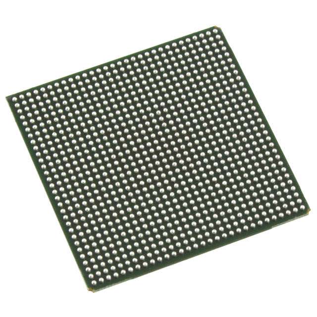
LFE2M100SE-7FN1152C
| Part Description |
ECP2M Field Programmable Gate Array (FPGA) IC 520 5435392 95000 1152-BBGA |
|---|---|
| Quantity | 862 Available (as of June 15, 2026) |

| Product Category | Field Programmable Gate Array (FPGA) |
|---|---|
| Manufacturer | Lattice Semiconductor Corporation |
| Manufacturing Status | Not For New Designs |
| Manufacturer Standard Lead Time | 20 Weeks |
| Datasheet |
Specifications & Environmental
| Device Package | 1152-FPBGA (35x35) | Grade | Commercial | Operating Temperature | 0°C – 85°C | ||
|---|---|---|---|---|---|---|---|
| Package / Case | 1152-BBGA | Number of I/O | 520 | Voltage | 1.14 V - 1.26 V | ||
| Mounting Method | Surface Mount | RoHS Compliance | ROHS3 Compliant | REACH Compliance | REACH Unaffected | ||
| Moisture Sensitivity Level | 3 (168 Hours) | Number of LABs/CLBs | 11875 | Number of Logic Elements/Cells | 95000 | ||
| Number of Gates | N/A | ECCN | 3A991D | HTS Code | 8542.39.0001 | ||
| Qualification | N/A | Total RAM Bits | 5435392 |
Overview of LFE2M100SE-7FN1152C – ECP2M Field Programmable Gate Array (FPGA) IC 520 5435392 95000 1152-BBGA
The LFE2M100SE-7FN1152C is a commercial-grade field programmable gate array (FPGA) from Lattice Semiconductor Corporation’s ECP2M family. It delivers a high logic capacity FPGA fabric with substantial embedded RAM and a large I/O count in a compact 1152-ball BGA package.
This device targets designs that require a balance of logic density, on-chip memory, and high I/O integration while operating within standard commercial temperature and low-voltage supply ranges.
Key Features
- Core Logic 95,000 logic elements provide programmable fabric for complex digital logic and custom accelerators.
- Embedded Memory Approximately 5.4 Mbits of on-chip RAM to support buffering, FIFOs, and packet processing without external memory.
- I/O Density 520 I/O pins accommodate broad peripheral interfacing and multi-channel signal connectivity.
- Power Supply Low-voltage operation with a supply range of 1.14 V to 1.26 V for core power optimization.
- Package and Mounting 1152-BBGA (supplier package 1152-FPBGA, 35 × 35 mm) in a surface-mount form factor for high-density PCB integration.
- Operating Range Commercial temperature grade with an operating range of 0 °C to 85 °C.
- Regulatory RoHS compliant for environmental and manufacturing compatibility.
Unique Advantages
- High logic capacity: 95,000 logic elements enable implementation of sizable custom logic and parallel processing functions on a single device.
- Significant on-chip memory: Approximately 5.4 Mbits of RAM reduces dependence on external memory, simplifying board design and improving latency for data buffering.
- Extensive I/O resources: 520 I/Os support multi-channel interfaces and a wide range of peripheral connections without additional IO expanders.
- Compact, high-density package: The 1152-ball BGA (35 × 35 mm) package delivers high pin count in a compact footprint for dense PCB layouts.
- Low-voltage core operation: 1.14 V to 1.26 V supply range supports power-conscious designs and aligns with modern low-voltage system architectures.
- Commercial temperature suitability: Rated 0 °C to 85 °C for standard commercial deployments and environments.
Why Choose LFE2M100SE-7FN1152C?
The LFE2M100SE-7FN1152C provides a balance of high logic density, ample embedded memory, and extensive I/O in a compact BGA package, making it well suited for commercial-grade designs that require integration and scalability. Its low-voltage core and RoHS compliance support modern power and manufacturing requirements, while the device’s specifications facilitate consolidation of functions to reduce BOM complexity.
Backed by Lattice Semiconductor Corporation, this FPGA is a practical choice for engineers and procurement teams seeking a high-capacity, commercially rated programmable device for complex digital designs and system integration.
Request a quote or submit an inquiry for pricing and availability for the LFE2M100SE-7FN1152C to discuss how this FPGA can meet your project requirements.