
LFE2M100SE-6FN1152I
| Part Description |
ECP2M Field Programmable Gate Array (FPGA) IC 520 5435392 95000 1152-BBGA |
|---|---|
| Quantity | 1,465 Available (as of October 8, 2026) |

| Product Category | Field Programmable Gate Array (FPGA) |
|---|---|
| Manufacturer | Lattice Semiconductor Corporation |
| Manufacturing Status | Not For New Designs |
| Manufacturer Standard Lead Time | 20 Weeks |
| Datasheet |
Specifications & Environmental
| Device Package | 1152-FPBGA (35x35) | Grade | Industrial | Operating Temperature | -40°C – 100°C | ||
|---|---|---|---|---|---|---|---|
| Package / Case | 1152-BBGA | Number of I/O | 520 | Voltage | 1.14 V - 1.26 V | ||
| Mounting Method | Surface Mount | RoHS Compliance | ROHS3 Compliant | REACH Compliance | REACH Unaffected | ||
| Moisture Sensitivity Level | 3 (168 Hours) | Number of LABs/CLBs | 11875 | Number of Logic Elements/Cells | 95000 | ||
| Number of Gates | N/A | ECCN | 3A991D | HTS Code | 8542.39.0001 | ||
| Qualification | N/A | Total RAM Bits | 5435392 |
Overview of LFE2M100SE-6FN1152I – ECP2M Field Programmable Gate Array (FPGA), 95,000 logic elements
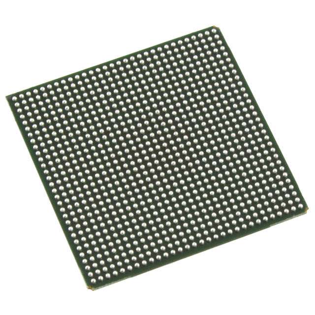
The LFE2M100SE-6FN1152I is an industrial-grade Field Programmable Gate Array (FPGA) from Lattice Semiconductor Corporation’s ECP2M family. It delivers high logic density, substantial embedded memory, and a large I/O count in a compact surface-mount BGA package.
Key hardware characteristics include approximately 95,000 logic elements, roughly 5.43 Mbits of on-chip RAM, 520 I/O pins, a 1152-BBGA package (1152-FPBGA, 35×35), a core voltage range of 1.14 V to 1.26 V, and an operating temperature range of −40 °C to 100 °C. The device is RoHS compliant and specified for industrial use.
Key Features
- Logic Capacity Approximately 95,000 logic elements for implementing complex digital functions and custom logic pipelines.
- Embedded Memory Approximately 5.43 Mbits of on-chip RAM (5,435,392 bits) to support buffering, packet storage, and state retention without external memory.
- I/O Density 520 I/O pins to accommodate multiple high-density interfaces and parallel peripherals.
- Package & Mounting 1152-BBGA package (supplier device package: 1152-FPBGA, 35×35) designed for surface-mount assembly in compact system layouts.
- Power Supply Core voltage supply range of 1.14 V to 1.26 V to match system power rails and designer requirements.
- Temperature & Grade Industrial grade with an operating temperature range of −40 °C to 100 °C for deployment in temperature-challenging environments.
- Regulatory Compliance RoHS compliant, supporting environmental and manufacturing requirements.
Typical Applications
- Industrial Control Used in industrial automation and control systems where industrial-grade temperature range and reliable on-chip resources are required.
- High-Density I/O Systems Ideal for designs that require many external interfaces or parallel connections, leveraging the 520 I/O pins for sensors, buses, and peripherals.
- Memory-Intensive Logic Suitable for applications that need significant on-chip buffering or packet storage, taking advantage of approximately 5.43 Mbits of embedded RAM.
- Compact Board Designs The 1152-BBGA surface-mount package supports space-constrained PCBs that benefit from high integration in a single FPGA device.
Unique Advantages
- High Logic Density: Approximately 95,000 logic elements allow complex functions and custom accelerators to be implemented on-chip, reducing external component count.
- Substantial On-Chip RAM: About 5.43 Mbits of embedded memory decreases reliance on external memory, simplifying board design and improving latency for buffering tasks.
- Extensive I/O Capacity: 520 I/O pins provide flexibility for connecting multiple peripherals, sensors, and high-speed interfaces without additional I/O expansion.
- Industrial Temperature Rating: Specified from −40 °C to 100 °C, supporting deployments in thermally demanding industrial environments.
- Compact BGA Packaging: 1152-BBGA (35×35) surface-mount package supports high-density, space-efficient layouts while maintaining robust electrical connections.
- RoHS Compliant: Meets RoHS requirements for environmentally conscious manufacturing and global market acceptance.
Why Choose LFE2M100SE-6FN1152I?
The LFE2M100SE-6FN1152I positions itself as a high-density, industrial-grade FPGA option that balances substantial logic resources, embedded memory, and broad I/O capability within a compact BGA footprint. It is well suited for engineers and system designers who need a single-device solution for complex logic, buffering, and high-pin-count I/O in industrial applications.
Backed by Lattice Semiconductor Corporation, this device offers defined electrical and thermal specifications—1.14 V to 1.26 V supply range and −40 °C to 100 °C operation—providing determinism for long-term deployments where known margins and compliance are important.
Request a quote or submit an inquiry to discuss availability, pricing, and how the LFE2M100SE-6FN1152I can fit your next industrial FPGA design.

























Date Founded: 1983
Headquarters: Hillsboro, Oregon, USA
Employees: 1,000+
Revenue: $627.7 Million
Certifications and Memberships: ISO9001:2015, ISO14001:2015, IATF16949:2016


