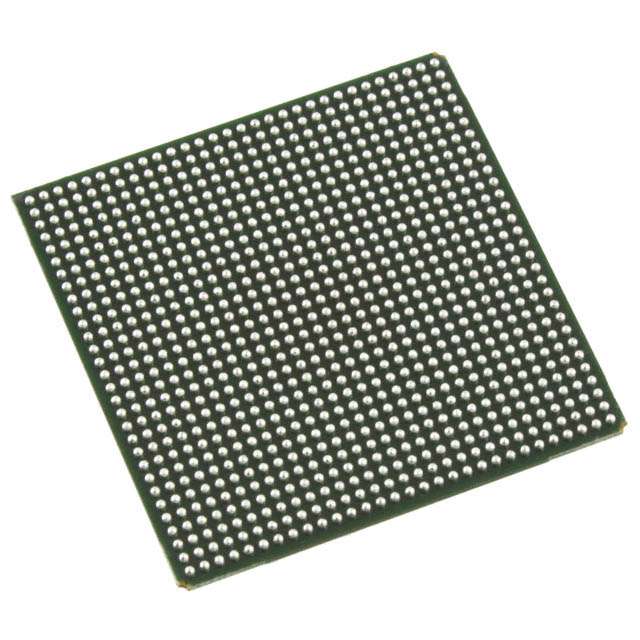
LFE2M100SE-6FN900C
| Part Description |
ECP2M Field Programmable Gate Array (FPGA) IC 416 5435392 95000 900-BBGA |
|---|---|
| Quantity | 444 Available (as of June 15, 2026) |

| Product Category | Field Programmable Gate Array (FPGA) |
|---|---|
| Manufacturer | Lattice Semiconductor Corporation |
| Manufacturing Status | Active |
| Manufacturer Standard Lead Time | 20 Weeks |
| Datasheet |
Specifications & Environmental
| Device Package | 900-FPBGA (31x31) | Grade | Commercial | Operating Temperature | 0°C – 85°C | ||
|---|---|---|---|---|---|---|---|
| Package / Case | 900-BBGA | Number of I/O | 416 | Voltage | 1.14 V - 1.26 V | ||
| Mounting Method | Surface Mount | RoHS Compliance | ROHS3 Compliant | REACH Compliance | REACH Unaffected | ||
| Moisture Sensitivity Level | 3 (168 Hours) | Number of LABs/CLBs | 11875 | Number of Logic Elements/Cells | 95000 | ||
| Number of Gates | N/A | ECCN | 3A991D | HTS Code | 8542.39.0001 | ||
| Qualification | N/A | Total RAM Bits | 5435392 |
Overview of LFE2M100SE-6FN900C – ECP2M FPGA, 95,000 Logic Elements, 416 I/Os, 900‑BGA
The LFE2M100SE-6FN900C is an ECP2M Field Programmable Gate Array (FPGA) IC from Lattice Semiconductor Corporation. It delivers a mid-range combination of programmable logic, on-chip memory, and a high I/O count in a compact 900‑ball BGA package.
With 95,000 logic elements, approximately 5.4 Mbits of embedded RAM and up to 416 I/Os, this device is suited for designs that require substantial logic density, on-chip buffering, and extensive peripheral connectivity within commercial temperature ranges.
Key Features
- Core Logic 95,000 logic elements provide substantial programmable capacity for complex combinational and sequential logic implementations.
- Embedded Memory Approximately 5.4 Mbits of on‑chip RAM for buffering, FIFOs, and local storage to support data‑intensive logic functions.
- I/O Density Up to 416 general-purpose I/Os to support multiple interfaces, parallel buses, and extensive external device connections.
- Package 900‑BBGA package (supplier package: 900‑FPBGA, 31×31 mm) for high pin‑count integration in space‑conscious board designs.
- Power Core supply voltage range of 1.14 V to 1.26 V to match low‑voltage system domains and optimize power delivery.
- Mounting & Compliance Surface mount device with RoHS compliance for modern manufacturing and environmental standards.
- Operating Range & Grade Commercial grade device rated for 0 °C to 85 °C operation.
Typical Applications
- Communications Equipment High I/O count and embedded memory enable protocol bridging, packet buffering, and custom interface logic.
- Industrial Control Programmable logic capacity supports complex control algorithms, real‑time decision logic, and multiple sensor or actuator interfaces.
- Measurement & Instrumentation On‑chip RAM and abundant I/Os facilitate data acquisition, buffering, and parallel sensor interfacing.
- Embedded Systems A dense logic fabric and significant embedded memory allow consolidation of custom peripherals and glue logic into a single device.
Unique Advantages
- High Logic Density: 95,000 logic elements reduce the need for multiple devices, simplifying board design and lowering BOM complexity.
- Significant On‑Chip Memory: Approximately 5.4 Mbits of embedded RAM supports buffering and local data processing without external memory.
- Extensive I/O Count: 416 I/Os provide flexibility to connect many peripherals or implement parallel interfaces without external multiplexing.
- Compact High‑Pin Package: 900‑BBGA (31×31 mm) enables high pin density in a space‑efficient footprint for compact systems.
- Low‑Voltage Core: 1.14–1.26 V supply range aligns with contemporary low‑voltage system domains to help optimize power delivery.
- RoHS Compliant: Meets environmental compliance expectations for commercial manufacturing.
Why Choose LFE2M100SE-6FN900C?
The LFE2M100SE-6FN900C positions itself as a capable mid‑range FPGA offering a blend of substantial logic capacity, meaningful embedded RAM, and a very high I/O count in a compact 900‑ball BGA package. It is well suited for designers seeking to consolidate custom logic, buffering, and interface functions into a single, surface‑mount device across commercial temperature conditions.
Manufactured by Lattice Semiconductor Corporation, this FPGA is appropriate for teams building communications, industrial control, instrumentation, and embedded systems that require a scalable, integrated logic solution with clear electrical and mechanical characteristics.
Request a quote or submit an inquiry to receive pricing, availability, and procurement details for the LFE2M100SE-6FN900C.