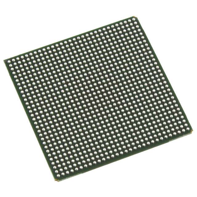
LFE2M100SE-7F900C
| Part Description |
ECP2M Field Programmable Gate Array (FPGA) IC 416 5435392 95000 900-BBGA |
|---|---|
| Quantity | 596 Available (as of June 15, 2026) |

| Product Category | Field Programmable Gate Array (FPGA) |
|---|---|
| Manufacturer | Lattice Semiconductor Corporation |
| Manufacturing Status | Obsolete |
| Manufacturer Standard Lead Time | Contact Us |
| Datasheet |
Specifications & Environmental
| Device Package | 900-FPBGA (31x31) | Grade | Commercial | Operating Temperature | 0°C – 85°C | ||
|---|---|---|---|---|---|---|---|
| Package / Case | 900-BBGA | Number of I/O | 416 | Voltage | 1.14 V - 1.26 V | ||
| Mounting Method | Surface Mount | RoHS Compliance | RoHS non-compliant | REACH Compliance | REACH Unaffected | ||
| Moisture Sensitivity Level | 3 (168 Hours) | Number of LABs/CLBs | 11875 | Number of Logic Elements/Cells | 95000 | ||
| Number of Gates | N/A | ECCN | 3A991D | HTS Code | 8542.39.0001 | ||
| Qualification | N/A | Total RAM Bits | 5435392 |
Overview of LFE2M100SE-7F900C – ECP2M Field Programmable Gate Array (FPGA), 900-BBGA
The LFE2M100SE-7F900C is an ECP2M family field programmable gate array (FPGA) supplied in a 900-BBGA package. It provides a high-density programmable fabric with 95,000 logic elements and approximately 5.4 Mbits of embedded memory to implement custom digital functions.
With 416 I/O and a commercial operating range, this device is suited for a wide range of embedded and communications-focused designs that require on-chip memory, flexible I/O, and compact surface-mount packaging.
Key Features
- Programmable Logic Capacity 95,000 logic elements for implementing complex digital logic and custom architectures.
- Embedded Memory Approximately 5.4 Mbits of on-chip RAM to support buffering, local data storage, and state machines.
- I/O Resources 416 available I/O pins to interface with peripherals, sensors, and high-density connectors.
- Power Supply Range Designed for VCC operation between 1.14 V and 1.26 V to match system power rails.
- Package and Mounting 900-BBGA package; supplier device package listed as 900-FPBGA (31x31). Surface-mount mounting type for board-level assembly.
- Operating Temperature Commercial grade operation from 0°C to 85°C.
- Standards Compliance RoHS-compliant construction for environmental regulatory alignment.
Typical Applications
- Embedded Systems: Implement glue logic, protocol bridging, and custom control functions where on-chip memory and programmable logic simplify board design.
- Communications & Networking: Use the device’s high I/O count and programmable fabric to handle interface aggregation, packet handling, or protocol adaptation.
- Video & Imaging Processing: Leverage the logic capacity and embedded RAM for buffering, pixel processing pipelines, and timing control.
- Test & Measurement Equipment: Apply the FPGA for real-time signal conditioning, custom data capture, and instrumentation control tasks.
Unique Advantages
- High Integration Density: 95,000 logic elements reduce the need for multiple discrete devices and simplify system architecture.
- Substantial On-Chip Memory: Approximately 5.4 Mbits of embedded RAM supports local data storage and lowers external memory requirements.
- Flexible I/O Count: 416 I/Os allow diverse peripheral interfacing and multi-channel system designs without extensive board-level multiplexing.
- Compact Surface-Mount Package: 900-BBGA (900-FPBGA 31x31) enables dense PCB layouts for space-constrained applications.
- Commercial Temperature Range: Rated 0°C to 85°C to match typical commercial product environments.
- RoHS Compliance: Environmentally compliant design for global product deployment.
Why Choose LFE2M100SE-7F900C?
The LFE2M100SE-7F900C balances high programmable logic capacity, on-chip memory, and abundant I/O in a compact 900-BBGA surface-mount package. Its specifications make it well suited for engineers building embedded systems, communications gear, and advanced processing modules that require a programmable, integrated solution within a commercial temperature range.
Choosing this FPGA supports designs that benefit from reduced external component count, flexible I/O mapping, and significant on-chip memory, offering a scalable platform for development and deployment across a range of commercial applications.
Request a quote or submit an RFQ to receive pricing and availability information for the LFE2M100SE-7F900C.