
M1A3P400-1FG144I
| Part Description |
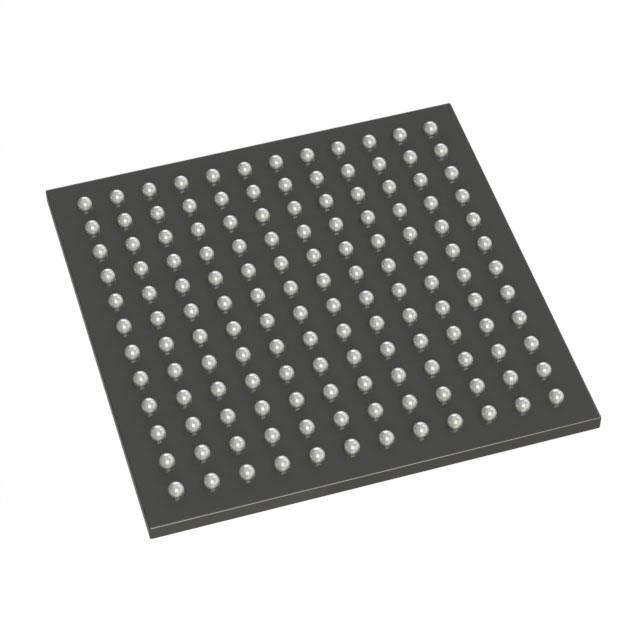
ProASIC3 Field Programmable Gate Array (FPGA) IC 97 55296 144-LBGA |
|---|---|
| Quantity | 313 Available (as of June 15, 2026) |
| Product Category | Field Programmable Gate Array (FPGA) |
|---|---|
| Manufacturer | Microchip Technology |
| Manufacturing Status | Active |
| Manufacturer Standard Lead Time | 12 Weeks |
| Datasheet |
Specifications & Environmental
| Device Package | 144-FPBGA (13x13) | Grade | Industrial | Operating Temperature | -40°C – 100°C | ||
|---|---|---|---|---|---|---|---|
| Package / Case | 144-LBGA | Number of I/O | 97 | Voltage | 1.425 V - 1.575 V | ||
| Mounting Method | Surface Mount | RoHS Compliance | RoHS non-compliant | REACH Compliance | REACH Unaffected | ||
| Moisture Sensitivity Level | 3 (168 Hours) | Number of LABs/CLBs | 9216 | Number of Logic Elements/Cells | 9216 | ||
| Number of Gates | 400000 | ECCN | 3A991D | HTS Code | 8542.39.0001 | ||
| Qualification | N/A | Total RAM Bits | 55296 |
Overview of M1A3P400-1FG144I – ProASIC3 Flash FPGA, 9,216 logic elements, 97 I/O, 144‑LBGA
The M1A3P400-1FG144I is a ProASIC3 family flash-based FPGA from Microchip Technology designed for programmable digital logic integration. It delivers 9,216 logic elements and approximately 400,000 gates with 55,296 bits of on-chip RAM to support a broad range of custom logic and interface functions.
Targeted at industrial applications and commercial embedded systems, this surface-mount device combines a compact 144-LBGA package with a 97-pin I/O count and a narrow supply voltage range for consistent, low-voltage operation across a −40 °C to 100 °C operating range.
Key Features
- Logic Capacity — 9,216 logic elements (9216 logic elements) and approximately 400,000 gates provide the silicon resources for complex custom logic and glue-logic implementations.
- On‑Chip Memory — 55,296 bits of embedded RAM for local buffering, state storage, and small data structures inside the FPGA design.
- I/O Count — 97 user I/O pins to support parallel interfaces, GPIO expansion, and mixed signal domain connections.
- Flash‑Based Architecture — Part of the ProASIC3 family with Flash*Freeze technology referenced in the device family documentation, providing nonvolatile configuration storage at power-up.
- Power and Voltage — Operates from a core supply of 1.425 V to 1.575 V for stable low-voltage core operation.
- Package and Mounting — 144‑LBGA (supplier package: 144‑FPBGA, 13 × 13 mm) in a surface-mount form factor to save PCB area while enabling high-density integration.
- Industrial Temperature Range — Rated for operation from −40 °C to 100 °C, suitable for industrial environments.
- RoHS Compliant — Conforms to RoHS environmental requirements.
Typical Applications
- Industrial Control — Implement custom state machines, I/O expansion, and deterministic control logic in factory automation and process control systems.
- Communications Equipment — Provide protocol glue logic, parallel interface handling, and custom datapath functions in telecom and network hardware.
- Aerospace & Defense Systems — Deploy configurable logic resources for mission-specific signal processing and control within the broader aerospace and defense market segments referenced in the device family documentation.
- Data Center and Enterprise Infrastructure — Use programmable logic for system management, custom interfacing, and hardware acceleration tasks in rack‑mount and appliance platforms.
Unique Advantages
- Compact BGA Packaging: 144‑LBGA (13 × 13 mm) saves PCB area while delivering substantial logic and I/O capability.
- High Integration Density: 9,216 logic elements and ~400,000 gates enable consolidation of multiple discrete functions into a single device, simplifying board-level design.
- On‑Chip Memory: 55,296 bits of embedded RAM reduce dependence on external memory for small buffers and state storage.
- Industrial Reliability: Rated for −40 °C to 100 °C operation and offered in a surface-mount package suitable for industrial system designs.
- Low‑Voltage Core: Narrow core supply range (1.425 V–1.575 V) supports consistent, controlled power delivery for the FPGA core.
- Environmental Compliance: RoHS compliance supports deployments where lead‑free and restricted substance requirements apply.
Why Choose M1A3P400-1FG144I?
The M1A3P400-1FG144I positions itself as a practical, flash-based programmable logic option for designers needing moderate logic density, a measurable on-chip RAM footprint, and a healthy I/O count in a compact BGA package. Its industrial temperature rating and RoHS compliance make it suitable for long-lived commercial and industrial applications where stable operation across a wide temperature range is required.
Engineering teams seeking to reduce board-level complexity while maintaining field-programmability and nonvolatile configuration storage will find the combination of logic resources, I/O, and package geometry useful for consolidating functions and simplifying system architectures.
Request a quote or submit a pricing inquiry to receive availability and lead-time information for the M1A3P400-1FG144I.


Date Founded: 1989
Headquarters: Chandler, Arizona, USA
Employees: 22,000+
Revenue: $8.349 Billion
Certifications and Memberships: ISO9001:2015, IATF16949:2016, AS 9100D


