
M1A3P400-1FG256I
| Part Description |
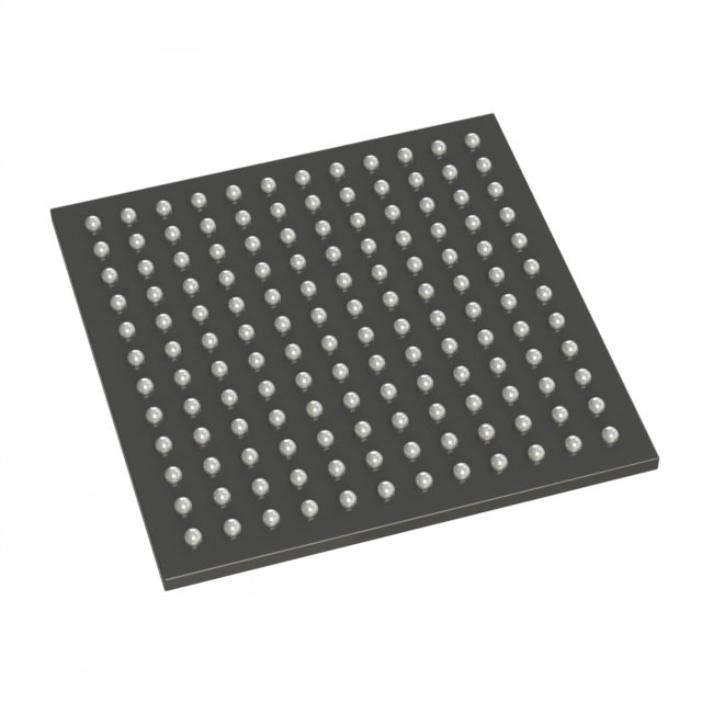
ProASIC3 Field Programmable Gate Array (FPGA) IC 178 55296 256-LBGA |
|---|---|
| Quantity | 557 Available (as of October 8, 2026) |

| Product Category | Field Programmable Gate Array (FPGA) |
|---|---|
| Manufacturer | Microchip Technology |
| Manufacturing Status | Active |
| Manufacturer Standard Lead Time | 12 Weeks |
| Datasheet |
Specifications & Environmental
| Device Package | 256-FPBGA (17x17) | Grade | Industrial | Operating Temperature | -40°C – 100°C | ||
|---|---|---|---|---|---|---|---|
| Package / Case | 256-LBGA | Number of I/O | 178 | Voltage | 1.425 V - 1.575 V | ||
| Mounting Method | Surface Mount | RoHS Compliance | RoHS non-compliant | REACH Compliance | REACH Unaffected | ||
| Moisture Sensitivity Level | 3 (168 Hours) | Number of LABs/CLBs | 9216 | Number of Logic Elements/Cells | 9216 | ||
| Number of Gates | 400000 | ECCN | 3A991D | HTS Code | 8542.39.0001 | ||
| Qualification | N/A | Total RAM Bits | 55296 |
Overview of M1A3P400-1FG256I – ProASIC3 Field Programmable Gate Array (FPGA) IC 400k-gate, 256-LBGA
The M1A3P400-1FG256I is a ProASIC3-series Flash FPGA offering a combination of programmable logic, embedded memory and a broad I/O complement in a compact 256‑LBGA package. As part of the ProASIC3/EL low-power flash FPGA family that incorporates Flash*Freeze technology, this device targets industrial embedded systems that require programmable logic with defined temperature and supply specifications.
Key silicon attributes include 9,216 logic elements (cells), approximately 55 Kbits of on-chip RAM, 178 user I/Os and a nominal logic capacity of 400,000 gates—delivered in a surface-mount 256‑LBGA (256‑FPBGA, 17×17) package.
Key Features
- Core Logic 9,216 logic elements (cells) providing a logic capacity of 400,000 gates for flexible implementation of custom logic and glue functions.
- Embedded Memory Approximately 55 Kbits of total on-chip RAM (55,296 bits) to support small buffers, FIFOs and register files without external memory.
- I/O Resources 178 user I/O pins to support wide interfacing options for parallel and serial peripheral connections.
- Low-Power Flash Technology Part of the ProASIC3/EL low-power flash FPGA family with Flash*Freeze technology for reduced power modes as described in the family datasheet.
- Power and Operating Range Single-supply operation within 1.425 V to 1.575 V and specified operating temperature range of −40 °C to 100 °C, suitable for industrial temperature environments.
- Package and Mounting Surface-mount 256‑LBGA package (supplier package: 256‑FPBGA, 17×17) for compact board-level integration.
- Compliance RoHS compliant to support environmentally conscious manufacturing requirements.
Typical Applications
- Industrial Embedded Systems Deploy programmable logic in industrial controllers and instrumentation where extended temperature support and a robust I/O count are required.
- Interface and Glue Logic Implement protocol bridging, bus consolidation and custom interfacing using the device’s abundant I/Os and on-chip logic.
- Low-Power FPGA Designs Leverage the ProASIC3/EL family’s low-power flash characteristics and Flash*Freeze capability for applications that benefit from reduced standby power.
Unique Advantages
- Well-defined industrial operating range: Specified −40 °C to 100 °C operation aligns the device with industrial-class deployments.
- High integration in a compact package: 9,216 logic elements and 178 I/Os packaged in a 256‑LBGA reduce board footprint and simplify routing.
- On-chip memory for reduced BOM: Approximately 55 Kbits of embedded RAM supports local buffering and control logic, minimizing external memory needs.
- Flash-based non-volatile configuration: ProASIC3/EL flash architecture enables in-system programmability without external configuration memory.
- Narrow supply window for predictable power design: 1.425 V to 1.575 V supply specification helps designers target predictable power rails and margins.
- RoHS compliant: Meets common lead-free manufacturing requirements for commercial and industrial production.
Why Choose M1A3P400-1FG256I?
The M1A3P400-1FG256I balances a substantial logic resource set and on-chip RAM with a significant I/O complement in a space-efficient 256‑LBGA package, making it suitable for industrial embedded designs that require programmable logic with defined temperature and supply constraints. Its inclusion in the ProASIC3/EL low-power flash FPGA family and support for Flash*Freeze technology provide designers with non-volatile configurability and low-power operation options.
This device is appropriate for customers seeking a flash-based FPGA with clear, verifiable specifications for logic density, memory, I/O count, package type and operating range—helpful for long-term designs where stability and predictable electrical/thermal behavior matter.
Request a quote or submit an inquiry to purchase the M1A3P400-1FG256I and receive detailed pricing and availability information for your project needs.
























Date Founded: 1989
Headquarters: Chandler, Arizona, USA
Employees: 22,000+
Revenue: $8.349 Billion
Certifications and Memberships: ISO9001:2015, IATF16949:2016, AS 9100D




