
M1A3P400-1FG256
| Part Description |
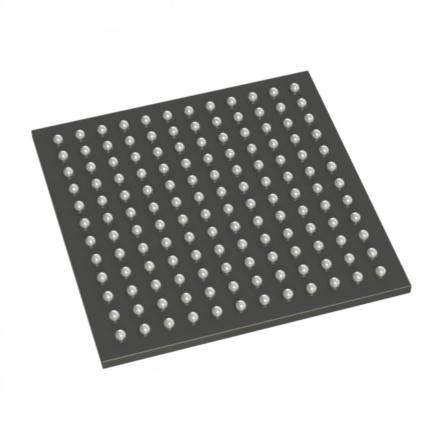
ProASIC3 Field Programmable Gate Array (FPGA) IC 178 55296 256-LBGA |
|---|---|
| Quantity | 169 Available (as of October 7, 2026) |

| Product Category | Field Programmable Gate Array (FPGA) |
|---|---|
| Manufacturer | Microchip Technology |
| Manufacturing Status | Active |
| Manufacturer Standard Lead Time | 12 Weeks |
| Datasheet |
Specifications & Environmental
| Device Package | 256-FPBGA (17x17) | Grade | Commercial | Operating Temperature | 0°C – 85°C | ||
|---|---|---|---|---|---|---|---|
| Package / Case | 256-LBGA | Number of I/O | 178 | Voltage | 1.425 V - 1.575 V | ||
| Mounting Method | Surface Mount | RoHS Compliance | RoHS non-compliant | REACH Compliance | REACH Unaffected | ||
| Moisture Sensitivity Level | 3 (168 Hours) | Number of LABs/CLBs | 9216 | Number of Logic Elements/Cells | 9216 | ||
| Number of Gates | 400000 | ECCN | 3A991D | HTS Code | 8542.39.0001 | ||
| Qualification | N/A | Total RAM Bits | 55296 |
Overview of M1A3P400-1FG256 – ProASIC3 Field Programmable Gate Array (FPGA) IC 178 55296 256-LBGA
The M1A3P400-1FG256 is a ProASIC3 flash-based FPGA from Microchip Technology offered in a 256-LBGA package. It integrates 9,216 logic elements and approximately 55,296 bits of on-chip RAM to implement custom digital logic, interface bridging, and control functions for commercial embedded systems.
This device provides a balanced combination of logic density, I/O count and low-voltage operation (1.425 V to 1.575 V) suited to communications, data and industrial-class designs that require reprogrammable logic in a compact surface-mount package. The device is RoHS compliant and rated for commercial temperature operation (0 °C to 85 °C).
Key Features
- Logic Capacity — 9,216 logic elements (cells) supporting up to 400,000 gates for implementing mid-density digital designs and glue logic.
- Embedded Memory — Approximately 0.055 Mbits (55,296 bits) of on-chip RAM for buffering, FIFOs and small data structures.
- I/O Resources — 178 available I/O pins to support multiple parallel interfaces and mixed-signal front-ends.
- Package and Mounting — 256-LBGA package (supplier package: 256-FPBGA, 17×17) in a surface-mount form factor for compact PCB integration.
- Supply Voltage — Operates from 1.425 V to 1.575 V, enabling integration with low-voltage system rails.
- Operating Grade — Commercial temperature range specified from 0 °C to 85 °C.
- Flash-based Architecture — Part of the ProASIC3 family with documented Flash*Freeze technology at the series level (flash-based configuration documented in the ProASIC3/EL datasheet).
- Regulatory — RoHS compliant for lead-free manufacturing processes.
Typical Applications
- Communications Equipment — Implement protocol bridging, packet pre-processing, and I/O adaptation using the device’s logic density and abundant I/O.
- Industrial Control — Deploy for machine control, sensor interfacing, and deterministic logic tasks within commercial-temperature industrial systems.
- Embedded Systems — Use as glue logic, custom peripheral controllers, or interface concentrators in compact, surface-mount designs.
Unique Advantages
- High Logic Density: 9,216 logic elements and 400,000 gates provide the capacity to implement complex finite-state machines and custom datapaths without external ASICs.
- Generous I/O Count: 178 I/O pins enable direct connection to multiple peripherals and parallel interfaces, reducing the need for external multiplexers or bridges.
- Compact, Manufacturable Package: The 256-LBGA (17×17) surface-mount footprint balances board space and pin count for compact system designs.
- Low-Voltage Operation: Supported supply range of 1.425 V to 1.575 V aligns with modern low-voltage system rails for power-efficient designs.
- RoHS Compliance: Meets lead-free manufacturing requirements for commercial production environments.
- Series-Level Flash Configuration: ProASIC3 family flash-based configuration (Flash*Freeze technology documented in the datasheet) supports non-volatile programming behavior at the family level.
Why Choose M1A3P400-1FG256?
The M1A3P400-1FG256 occupies a valuable position for designers seeking a mid-density, flash-based FPGA with substantial I/O and compact packaging. Its combination of 9,216 logic elements, 178 I/Os and on-chip RAM makes it suitable for embedded and communications-oriented designs that need reprogrammable logic without large board-level overhead.
With commercial temperature grading, RoHS compliance and a low-voltage supply range, this device delivers a pragmatic balance of integration, manufacturability and predictable electrical characteristics for production systems that leverage the ProASIC3 architecture.
Request a quote or submit a sales inquiry to begin procurement or to get pricing, lead-time and availability information for the M1A3P400-1FG256.
























Date Founded: 1989
Headquarters: Chandler, Arizona, USA
Employees: 22,000+
Revenue: $8.349 Billion
Certifications and Memberships: ISO9001:2015, IATF16949:2016, AS 9100D




