
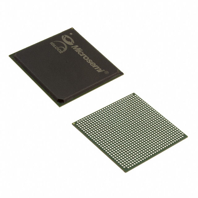
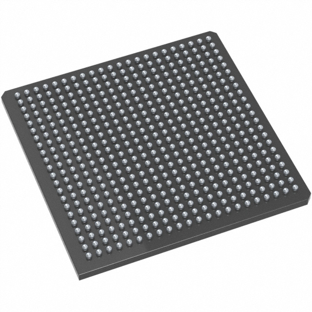
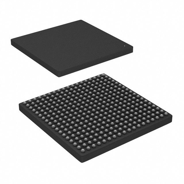
M2GL050TS-1FG484M
| Part Description |
IGLOO2 Field Programmable Gate Array (FPGA) IC 267 1869824 56340 484-BGA |
|---|---|
| Quantity | 564 Available (as of June 15, 2026) |

| Product Category | Field Programmable Gate Array (FPGA) |
|---|---|
| Manufacturer | Microchip Technology |
| Manufacturing Status | Active |
| Manufacturer Standard Lead Time | 16 Weeks |
| Datasheet |
Specifications & Environmental
| Device Package | 484-FPBGA (23x23) | Grade | Military | Operating Temperature | -55°C – 125°C | ||
|---|---|---|---|---|---|---|---|
| Package / Case | 484-BGA | Number of I/O | 267 | Voltage | 1.14 V - 2.625 V | ||
| Mounting Method | Surface Mount | RoHS Compliance | RoHS non-compliant | REACH Compliance | REACH Unaffected | ||
| Moisture Sensitivity Level | 3 (168 Hours) | Number of LABs/CLBs | 56340 | Number of Logic Elements/Cells | 56340 | ||
| Number of Gates | N/A | ECCN | 3A001A2C | HTS Code | 8542.39.0001 | ||
| Qualification | MIL-STD-883 | Total RAM Bits | 1869824 |
Overview of M2GL050TS-1FG484M – IGLOO2 Field Programmable Gate Array (FPGA), 484-BGA, Military Grade
The M2GL050TS-1FG484M is an IGLOO2 Field Programmable Gate Array (FPGA) IC from Microchip Technology, delivered in a 484-FPBGA (23×23) package for surface-mount applications. It offers high logic density and on-chip embedded memory alongside a large I/O count, making it suitable for designs that require reprogrammable logic in military-qualified hardware.
With 56,340 logic elements, approximately 1.87 Mbits of embedded memory and 267 I/O pins, this device targets applications that demand substantial logic resources, extensive connectivity, and rugged environmental performance, including MIL-STD-883 qualification and extended temperature operation.
Key Features
- Logic Capacity Provides 56,340 logic elements for implementing complex logic, state machines, and custom processing pipelines.
- Embedded Memory Includes approximately 1.87 Mbits of on-chip RAM to support frame buffering, lookup tables, and local data storage without external memory.
- I/O and Connectivity Offers 267 I/O pins to support dense peripheral interfacing, multi-channel data paths, and flexible board-level routing.
- Power Supply Range Operates across a wide supply range from 1.14 V to 2.625 V to accommodate various system power architectures.
- Package and Mounting Supplied in a 484-FPBGA (23×23) package for surface-mount assembly, enabling compact board layouts.
- Military Qualification and Environmental Range Rated as Military grade with MIL-STD-883 qualification and an operating temperature range of −55 °C to 125 °C for deployment in harsh environments.
- RoHS Compliant Manufactured to meet RoHS environmental requirements.
Typical Applications
- Military and Defense Systems Used in mission-critical FPGA roles where MIL-STD-883 qualification and extended temperature operation are required.
- Rugged Embedded Control Suitable for embedded controllers and signal processing in environments demanding wide temperature tolerance and high logic density.
- Communications and Networking Equipment Supports protocol handling, packet processing, and I/O aggregation with its high logic count and large number of I/Os.
- Secure and Specialized Electronics Applicable to systems that require reconfigurable logic with on-chip RAM and extensive connectivity within a military-grade package.
Unique Advantages
- High Logic Integration: 56,340 logic elements enable consolidation of multiple functions into a single FPGA, reducing board-level complexity.
- Significant On-Chip Memory: Approximately 1.87 Mbits of embedded RAM provides local storage for buffering and deterministic data handling without immediate reliance on external memory.
- Extensive I/O Count: 267 I/Os facilitate direct interfacing with numerous peripherals, sensors, and high-density connectors.
- Military-Grade Reliability: MIL-STD-883 qualification and −55 °C to 125 °C operation support deployment in demanding environments and harsh conditions.
- Flexible Power Envelope: Wide supply range from 1.14 V to 2.625 V accommodates a variety of power domain designs and helps integrate with diverse system voltages.
- Compact Surface-Mount Package: 484-FPBGA (23×23) enables high-density PCB designs while providing substantial I/O and silicon in a single footprint.
Why Choose M2GL050TS-1FG484M?
The M2GL050TS-1FG484M positions itself as a military-grade FPGA solution combining high logic capacity, ample embedded memory and a large I/O complement within a compact 484-FPBGA package. It is tailored for engineers and procurement teams building rugged, reconfigurable systems that require MIL-STD-883 qualification and extended temperature performance.
Backed by Microchip Technology's IGLOO2 family, this device is a practical choice for developers needing scalable logic resources, robust environmental tolerance and flexible power compatibility in applications where reliability and field programmability are essential.
Request a quote or submit a procurement inquiry to obtain pricing, availability and ordering information for the M2GL050TS-1FG484M.


Date Founded: 1989
Headquarters: Chandler, Arizona, USA
Employees: 22,000+
Revenue: $8.349 Billion
Certifications and Memberships: ISO9001:2015, IATF16949:2016, AS 9100D


