
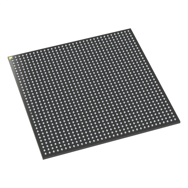
M2GL150T-FCS536I
| Part Description |
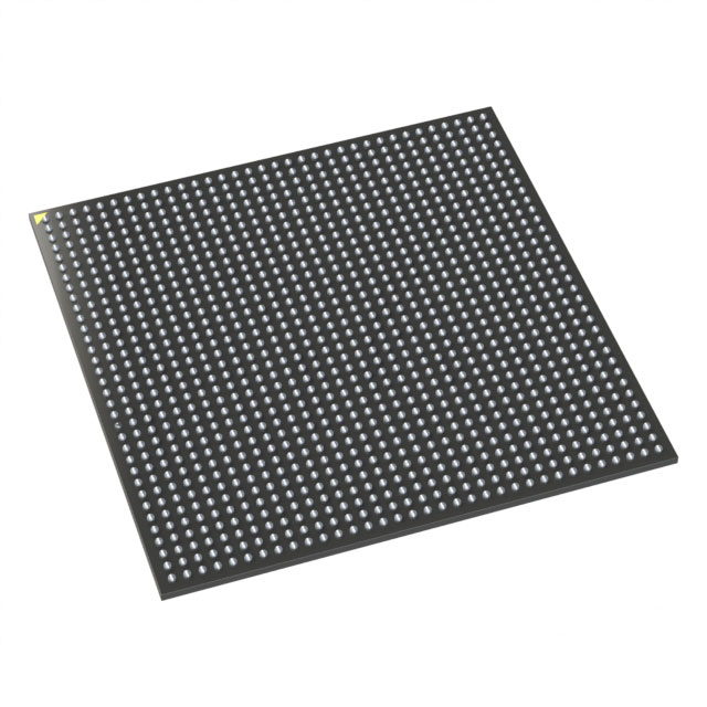
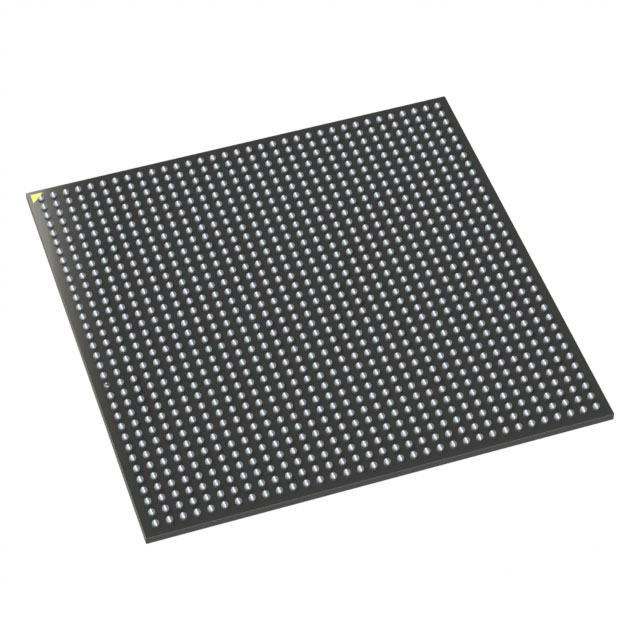
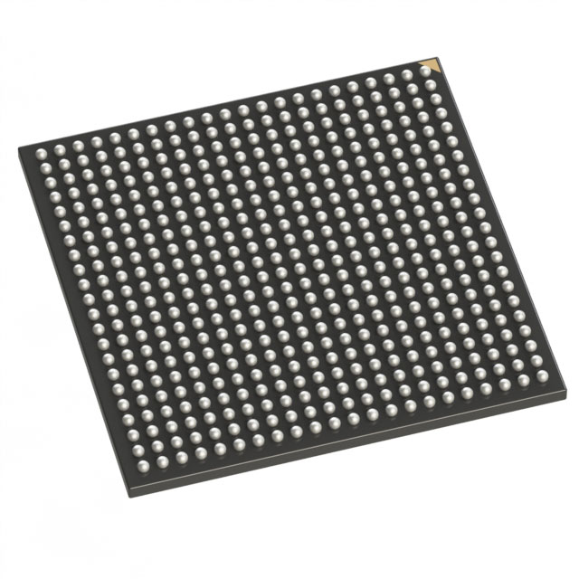
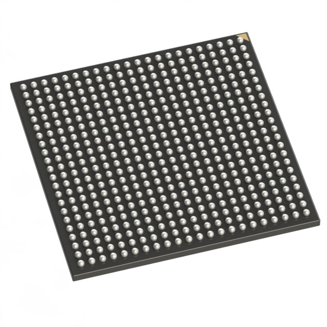
IGLOO2 Field Programmable Gate Array (FPGA) IC 293 5120000 146124 536-LFBGA, CSPBGA |
|---|---|
| Quantity | 1,481 Available (as of October 8, 2026) |

| Product Category | Field Programmable Gate Array (FPGA) |
|---|---|
| Manufacturer | Microchip Technology |
| Manufacturing Status | Active |
| Manufacturer Standard Lead Time | 10 Weeks |
| Datasheet |
Specifications & Environmental
| Device Package | 536-CSPBGA (16x16) | Grade | Industrial | Operating Temperature | -40°C – 100°C | ||
|---|---|---|---|---|---|---|---|
| Package / Case | 536-LFBGA, CSPBGA | Number of I/O | 293 | Voltage | 1.14 V - 2.625 V | ||
| Mounting Method | Surface Mount | RoHS Compliance | RoHS non-compliant | REACH Compliance | REACH Unaffected | ||
| Moisture Sensitivity Level | 3 (168 Hours) | Number of LABs/CLBs | 146124 | Number of Logic Elements/Cells | 146124 | ||
| Number of Gates | N/A | ECCN | 3A991B2 | HTS Code | 8542.39.0001 | ||
| Qualification | N/A | Total RAM Bits | 5120000 |
Overview of M2GL150T-FCS536I – IGLOO2 Field Programmable Gate Array (FPGA)
The M2GL150T-FCS536I is an IGLOO2 Field Programmable Gate Array (FPGA) IC offering high logic capacity and embedded memory in a compact CSPBGA package. It combines 146,124 logic elements with approximately 5.12 Mbits of embedded memory and 293 I/O pins to support dense digital designs.
Designed for industrial applications, this surface-mount FPGA operates across a wide supply voltage range (1.14 V to 2.625 V) and an industrial temperature range (−40 °C to 100 °C), providing a balanced platform for embedded control, data processing, and I/O consolidation in space-constrained systems.
Key Features
- Logic Capacity 146,124 logic elements provide substantial programmable logic resources for complex digital functions and custom logic implementation.
- Embedded Memory Approximately 5.12 Mbits of on-chip RAM to store buffers, state, and intermediate data without external memory.
- I/O Density 293 I/O pins support extensive external interfacing for sensors, peripherals, and multi-channel connectivity.
- Power Supply Flexibility Operates from 1.14 V to 2.625 V, enabling integration with a variety of system power architectures.
- Package & Mounting 536-LFBGA (536-CSPBGA, 16 × 16) surface-mount package for compact board-level implementation and high pin count in a small footprint.
- Industrial Temperature Range Rated for −40 °C to 100 °C operation, suitable for industrial and ruggedized environments.
- Regulatory Compliance RoHS compliant, supporting environmentally conscious manufacturing and assembly.
Typical Applications
- Industrial Control Use the FPGA’s high logic density and wide temperature range for motor control, PLC extensions, and real-time control logic in industrial systems.
- Data Acquisition & Processing On-chip memory and abundant logic elements enable buffering, preprocessing, and custom signal processing for sensor and measurement systems.
- Communications & I/O Aggregation A high I/O count supports protocol conversion, interface bridging, and aggregation of multiple serial or parallel channels.
- Embedded Prototyping & Custom Logic Compact package and flexible supply voltage make it suitable for board-level prototypes and integration into space-constrained embedded products.
Unique Advantages
- High Logic Integration: 146,124 logic elements reduce the need for multiple discrete chips when implementing complex custom logic functions.
- Substantial On-Chip Memory: Approximately 5.12 Mbits of embedded RAM allows internal buffering and state storage without relying on external memory.
- Extensive I/O Capacity: 293 I/O pins enable direct connections to numerous peripherals and sensors, simplifying board-level design.
- Compact High-Pin Package: 536-CSPBGA (16×16) package delivers a high pin count in a small footprint for dense PCB layouts.
- Industrial-Grade Operation: Rated for −40 °C to 100 °C, allowing deployment in a wide range of environmental conditions.
- Design Flexibility: Wide supply voltage range (1.14 V–2.625 V) supports integration with diverse power domains and system architectures.
Why Choose M2GL150T-FCS536I?
The M2GL150T-FCS536I positions itself as a versatile FPGA for engineers who require a combination of high logic density, meaningful on-chip memory, and a large number of I/Os in a compact, surface-mount package. Its industrial temperature rating and flexible supply voltage make it practical for robust embedded and control applications.
This device is well suited to designs that need to consolidate digital functions, implement custom processing pipelines, or handle multiple peripheral interfaces while maintaining a small board footprint. RoHS compliance further supports modern manufacturing requirements.
Request a quote or submit an RFQ for the M2GL150T-FCS536I to discuss pricing, availability, and lead times for your project requirements.




















Date Founded: 1989
Headquarters: Chandler, Arizona, USA
Employees: 22,000+
Revenue: $8.349 Billion
Certifications and Memberships: ISO9001:2015, IATF16949:2016, AS 9100D




