
XC2S600E-6FGG456C
| Part Description |
Spartan®-IIE Field Programmable Gate Array (FPGA) IC 329 294912 15552 456-BBGA |
|---|---|
| Quantity | 263 Available (as of June 15, 2026) |

| Product Category | Field Programmable Gate Array (FPGA) |
|---|---|
| Manufacturer | AMD |
| Manufacturing Status | Obsolete |
| Manufacturer Standard Lead Time | Contact Us |
| Datasheet |
Specifications & Environmental
| Device Package | 456-FBGA (23x23) | Grade | Commercial | Operating Temperature | 0°C – 85°C | ||
|---|---|---|---|---|---|---|---|
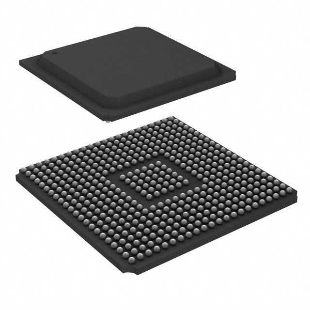
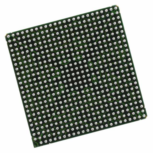
| Package / Case | 456-BBGA | Number of I/O | 329 | Voltage | 1.71 V - 1.89 V | ||
| Mounting Method | Surface Mount | RoHS Compliance | Unknown | REACH Compliance | REACH Unaffected | ||
| Moisture Sensitivity Level | 3 (168 Hours) | Number of LABs/CLBs | 3456 | Number of Logic Elements/Cells | 15552 | ||
| Number of Gates | 600000 | ECCN | 3A001A7A | HTS Code | 8542.39.0001 | ||
| Qualification | N/A | Total RAM Bits | 294912 |
Overview of XC2S600E-6FGG456C – Spartan®-IIE FPGA 456-BBGA
The XC2S600E-6FGG456C is a Spartan®-IIE field-programmable gate array (FPGA) in a 456-ball BGA package designed for cost-sensitive, reprogrammable digital logic applications. It combines a large logic resource pool with on-chip memory and flexible I/O to support system-level integration and iterative design updates.
As part of the Spartan-IIE family, the device offers architecture features and system-level capabilities intended as an alternative to mask-programmed ASICs, including in-system reprogrammability and support for high-performance interfaces.
Key Features
- Core Logic 15,552 logic elements (cells) and an architecture providing up to 600,000 system gates for complex digital functions.
- Embedded Memory Approximately 0.29 Mbits of on-chip RAM (294,912 total RAM bits) enabling both distributed and block RAM implementations.
- I/O Capacity 329 I/O pins to support a wide range of external interfaces and signal routing requirements.
- Clocking and Timing Family-level features include four dedicated delay-locked loops (DLLs) and multiple low-skew global clock nets for advanced clock control and timing management.
- Packaging and Mounting Surface-mount 456-ball BGA package (supplier device package: 456-FBGA, 23×23) for compact board-level integration.
- Power Core supply range 1.71 V to 1.89 V, suitable for the device’s specified operating conditions.
- Operating Range and Grade Commercial grade with an operating temperature range of 0 °C to 85 °C.
- Standards and Family Capabilities Series-level support includes numerous selectable I/O standards, block and distributed RAM structures, and family footprint compatibility across packages.
- Compliance RoHS compliant for lead-free assembly environments.
Typical Applications
- ASIC replacement and prototyping Used as a reprogrammable alternative to mask-programmed ASICs to reduce upfront development cost and enable field updates.
- High-speed interface bridging Supports designs requiring fast interfaces to external memory and peripherals, leveraging the device’s embedded RAM and I/O capacity.
- PCI and bus-interface designs Series-level features cite full 3.3 V PCI compliance and CardBus compatibility for bus-attached system designs.
- System control and glue logic Provides programmable logic, registers, and dedicated carry logic for control, data path, and arithmetic functions within larger systems.
Unique Advantages
- Highly integrated logic and memory: Large logic element count combined with approximately 0.29 Mbits of on-chip RAM reduces external component count and simplifies board design.
- Flexible I/O and interfacing: 329 I/Os and family support for many selectable I/O standards enable direct interfacing to diverse peripherals and signaling standards.
- Field reprogrammability: In-system reprogrammability lets designs be updated in the field without hardware replacement, shortening product cycles and enabling post-deployment fixes or enhancements.
- Advanced clock control: Multiple DLLs and low-skew global clock resources support complex timing schemes and help manage clock distribution across the design.
- Compact surface-mount packaging: 456-ball BGA (23×23) provides a high-density footprint for space-constrained PCBs while supporting modern assembly processes.
- Regulatory and assembly readiness: RoHS compliance supports lead-free manufacturing requirements.
Why Choose XC2S600E-6FGG456C?
The XC2S600E-6FGG456C positions itself as a cost-effective, reprogrammable solution for designs that require substantial logic resources, embedded memory, and flexible I/O in a compact BGA footprint. With a large logic element count, significant on-chip RAM, and family-level features such as DLLs and multiple I/O standards, it addresses designs that benefit from iterative development and in-field updates.
This commercial-grade Spartan®-IIE device is appropriate for engineers and teams building prototypes, system controllers, and interface logic that prioritize integration, reprogrammability, and compact packaging while operating within the specified voltage and temperature ranges.
Request a quote or submit an inquiry to get pricing and availability for the XC2S600E-6FGG456C and to discuss how it can fit into your next FPGA-based design.


Date Founded: 1969
Headquarters: Santa Clara, California, USA
Employees: 25,000+
Revenue: $22.68 Billion
Certifications and Memberships: ISO9001:2015, RoHS, REACH


