
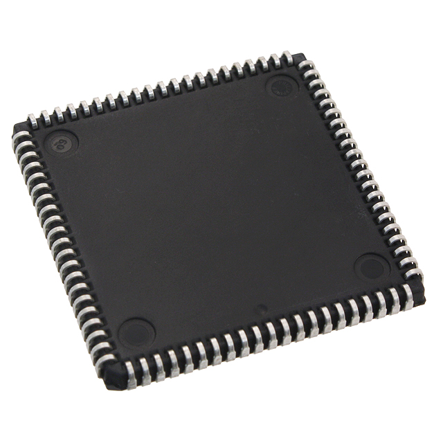
XC3142-3TQ100C
| Part Description |
XC3100 Field Programmable Gate Array (FPGA) IC 82 30784 144 100-LQFP |
|---|---|
| Quantity | 1,197 Available (as of October 8, 2026) |

| Product Category | Field Programmable Gate Array (FPGA) |
|---|---|
| Manufacturer | AMD |
| Manufacturing Status | Active |
| Manufacturer Standard Lead Time | 1 Weeks |
| Datasheet |
Specifications & Environmental
| Device Package | 100-TQFP (14x14) | Grade | Commercial | Operating Temperature | 0°C – 85°C | ||
|---|---|---|---|---|---|---|---|
| Package / Case | 100-LQFP | Number of I/O | 82 | Voltage | 4.75 V - 5.25 V | ||
| Mounting Method | Surface Mount | RoHS Compliance | RoHS non-compliant | REACH Compliance | REACH Unaffected | ||
| Moisture Sensitivity Level | 3 (168 Hours) | Number of LABs/CLBs | 144 | Number of Logic Elements/Cells | 144 | ||
| Number of Gates | 3000 | ECCN | EAR99 | HTS Code | 8542.39.0001 | ||
| Qualification | N/A | Total RAM Bits | 30784 |
Overview of XC3142-3TQ100C – XC3100 Field Programmable Gate Array (FPGA) IC 82 30784 144 100-LQFP
The XC3142-3TQ100C is a field programmable gate array (FPGA) packaged in a 100-pin LQFP/TQFP footprint designed for commercial-grade embedded logic applications. It provides a compact combination of programmable logic, embedded RAM and a substantial I/O count for small to medium-scale digital functions.
With 144 logic elements, about 30.8 kbits of on-chip RAM and 82 user I/O pins, this device is suited for designers needing modest programmable logic capacity in a surface-mount 100-pin package operating from a 4.75 V to 5.25 V supply and a 0 °C to 85 °C temperature range.
Key Features
- Logic Capacity — 144 logic elements (LEs) providing programmable resources for implementing custom digital functions and control logic.
- Embedded Memory — 30,784 bits of on-chip RAM (approximately 30.8 kbits) for data buffering, state storage and small lookup tables.
- I/O Resources — 82 user I/O pins, enabling broad interfacing to peripherals, sensors and external logic devices.
- Gate Equivalent — Approximately 3,000 gates of logic capacity for glue logic, protocol handling and peripheral control.
- Power Supply — Operates from a 4.75 V to 5.25 V supply, compatible with standard 5 V digital systems.
- Package and Mounting — Available in a 100-pin LQFP package; supplier device package listed as 100-TQFP (14×14). Surface-mount mounting for PCB assembly.
- Commercial Temperature Grade — Rated for 0 °C to 85 °C operation for general-purpose commercial applications.
- RoHS Compliant — Meets RoHS environmental requirements.
Typical Applications
- Glue Logic and System Integration — Implement custom interfacing, signal routing and control logic between discrete components and microcontrollers.
- Peripheral and Sensor Interfacing — Manage multiple I/O lines and small data buffers for sensor aggregation, digital filtering or protocol conversion.
- User Interface Control — Drive and coordinate buttons, LEDs, displays and simple input/output subsystems requiring moderate logic and I/O counts.
- Prototyping and Educational Projects — Suitable for early-stage development and learning where a compact, surface-mount FPGA with modest resources is required.
Unique Advantages
- Compact Programmability: 144 logic elements provide a programmable alternative to fixed-function glue logic, reducing discrete IC count and simplifying board design.
- On-Chip Memory: Approximately 30.8 kbits of embedded RAM enables local buffering and state storage without external memory, lowering BOM and board complexity.
- Generous I/O Count: 82 I/O pins allow flexible interfacing with sensors, peripherals and external buses within a single device.
- Standard 5 V Supply Compatibility: Operates from 4.75 V to 5.25 V for easy integration into existing 5 V digital systems and legacy designs.
- Surface-Mount 100-Pin Package: 100-LQFP / 100-TQFP (14×14) packaging balances pin density and assembly convenience for compact PCB layouts.
- Commercial Temperature Rating: Rated 0 °C to 85 °C for consistent operation in general-purpose commercial environments.
Why Choose XC3142-3TQ100C?
The XC3142-3TQ100C positions itself as a practical, compact FPGA option for designs that require moderate programmable logic, embedded RAM and a substantial I/O complement in a 100-pin surface-mount package. Its 144 logic elements, roughly 30.8 kbits of on-chip RAM and 82 I/O pins deliver the integration needed to replace multiple discrete components and streamline board-level designs.
This device is well suited to engineers developing commercial-grade embedded systems, board-level glue logic, I/O expansion and small-scale prototyping where 5 V supply compatibility, RoHS compliance and a standard temperature range are required. It offers a balance of integration and simplicity for projects targeting reliable, repeatable deployments.
Request a quote or submit an inquiry to receive pricing and availability information for the XC3142-3TQ100C.























Date Founded: 1969
Headquarters: Santa Clara, California, USA
Employees: 25,000+
Revenue: $22.68 Billion
Certifications and Memberships: ISO9001:2015, RoHS, REACH











