
XC4085XLA-09BGG352C
| Part Description |
XC4000XLA/XV Field Programmable Gate Array (FPGA) IC |
|---|---|
| Quantity | 296 Available (as of June 15, 2026) |
| Product Category | Field Programmable Gate Array (FPGA) |
|---|---|
| Manufacturer | AMD |
| Manufacturing Status | Active |
| Manufacturer Standard Lead Time | 1 Weeks |
| Datasheet |
Specifications & Environmental
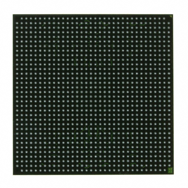
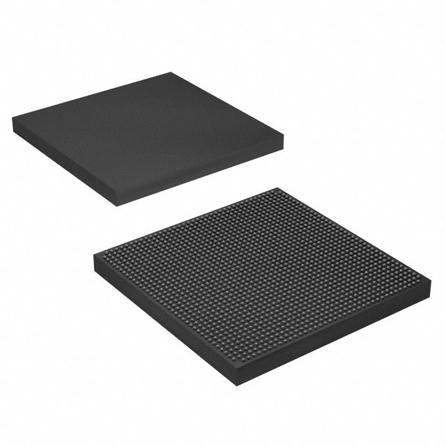
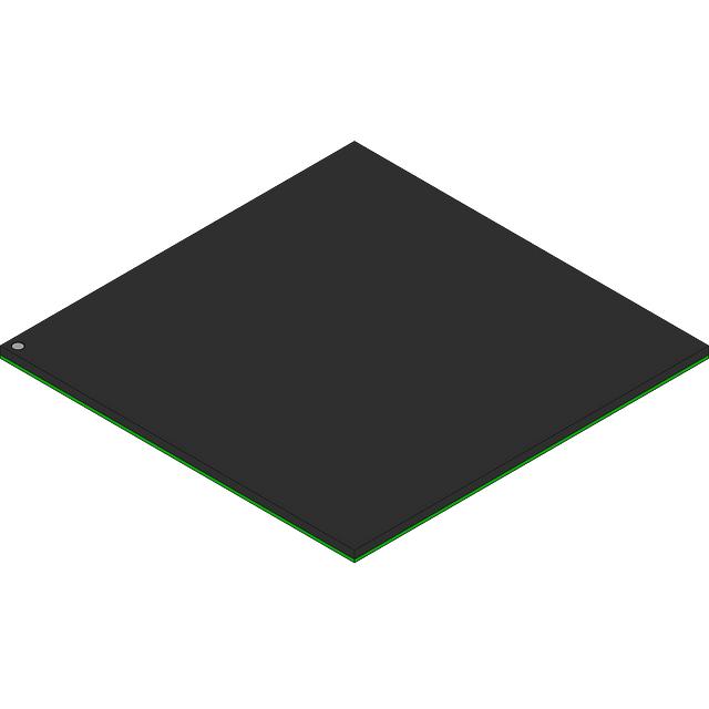
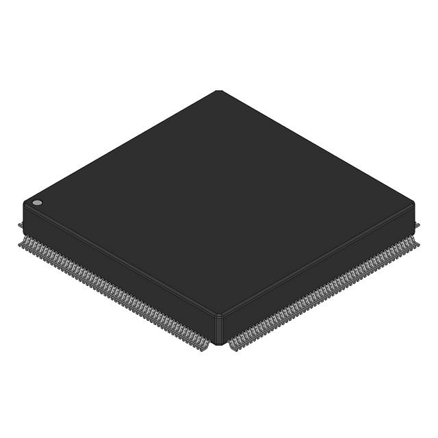
| Device Package | 352-MBGA (35x35) | Grade | Commercial | Operating Temperature | 0°C – 85°C | ||
|---|---|---|---|---|---|---|---|
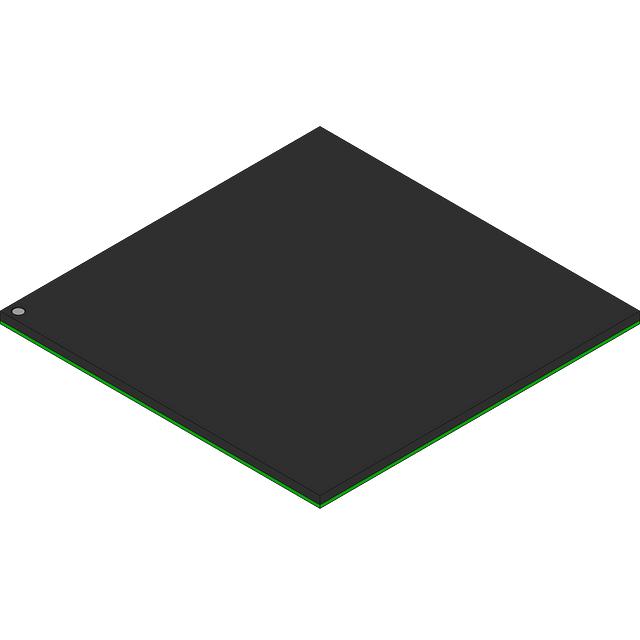
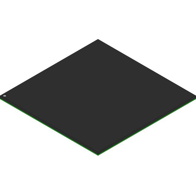
| Package / Case | 352-LBGA Exposed Pad, Metal | Number of I/O | 268 | Voltage | 3 V - 3.6 V | ||
| Mounting Method | Surface Mount | RoHS Compliance | ROHS3 Compliant | REACH Compliance | REACH Unaffected | ||
| Moisture Sensitivity Level | 3 (168 Hours) | Number of LABs/CLBs | 3136 | Number of Logic Elements/Cells | 7448 | ||
| Number of Gates | 55000 | ECCN | 3A991D | HTS Code | 8542.39.0001 | ||
| Qualification | N/A | Total RAM Bits | 100352 |
Overview of XC4085XLA-09BGG352C – XC4000XLA/XV Field Programmable Gate Array (FPGA) IC
The XC4085XLA-09BGG352C is a Field Programmable Gate Array (FPGA) IC in the XC4000XLA/XV family from AMD. It delivers a mid-range programmable logic resource set with on-chip memory and a high I/O count suitable for board-level integration in commercial electronic designs.
Designed for surface-mount assembly in a 352-ball BGA package, the device combines approximately 7,448 logic elements, about 0.10 Mbits of embedded RAM, and 268 general-purpose I/O for implementing custom digital logic, interface bridging, and system control functions within a 3.0 V to 3.6 V supply range.
Key Features
- Logic Capacity Approximately 7,448 logic elements and 3,136 configurable logic blocks (CLBs) provide the programmable fabric required for implementing complex digital functions.
- Embedded Memory Approximately 0.10 Mbits (100,352 bits) of on-chip RAM for data buffering, state storage, and small FIFO implementations.
- I/O Density 268 I/O pins support a wide range of external interfaces and parallel connections, enabling flexible system-level integration.
- Gate Count Equivalent to 55,000 gates of logic capacity for mapping combinational and sequential designs.
- Power and Supply Operates from a 3.0 V to 3.6 V supply domain suitable for common commercial power rails.
- Package and Mounting 352-LBGA exposed pad, metal package (supplier package: 352-MBGA 35×35) optimized for surface-mount PCB assembly and thermal conduction.
- Operating Range Commercial operating temperature range of 0 °C to 85 °C for standard commercial applications.
- RoHS Compliant Manufactured in compliance with RoHS requirements.
Typical Applications
- Custom Digital Logic Implement glue logic, protocol converters, and custom state machines using the device's 7,448 logic elements and CLB resources.
- Peripheral and Interface Control Handle parallel interfaces and multiple peripherals with 268 available I/O pins for direct board-level connections.
- Embedded System Integration Use the on-chip RAM and programmable fabric for buffering, control sequencing, and small-scale data handling within commercial embedded products.
Unique Advantages
- Balanced Logic and Memory Mix: The combination of ~7,448 logic elements and ~0.10 Mbits of RAM supports both control logic and modest data buffering in a single device, reducing BOM count.
- High I/O Count: 268 I/O pins enable direct interfacing to multiple peripherals and buses, simplifying board routing and system architecture.
- Compact BGA Package: The 352-LBGA exposed pad package provides a high-density footprint with thermal conduction suited for surface-mount assembly.
- Commercial Temperature Grade: Rated for 0 °C to 85 °C operation for mainstream commercial product deployments.
- Standard Supply Voltage: 3.0 V to 3.6 V supply compatibility aligns with common commercial digital power rails.
- RoHS Compliance: Environmentally compliant manufacturing supports regulatory needs for commercial products.
Why Choose XC4085XLA-09BGG352C?
The XC4085XLA-09BGG352C positions as a commercially graded, mid-range FPGA offering a pragmatic balance of logic elements, embedded memory, and a high I/O count in a compact 352-ball BGA package. Its specification set supports designers who need programmable logic and modest on-chip RAM for control, interface, and system integration tasks while keeping PCB footprint and component count under control.
This part is suited to development teams and product engineers building commercial electronic equipment that requires flexible digital implementation, direct peripheral interfacing, and surface-mount assembly. Its RoHS compliance and standard voltage operation help simplify procurement and power-domain design decisions.
Request a quote or submit your procurement inquiry to receive pricing and availability details for the XC4085XLA-09BGG352C.


Date Founded: 1969
Headquarters: Santa Clara, California, USA
Employees: 25,000+
Revenue: $22.68 Billion
Certifications and Memberships: ISO9001:2015, RoHS, REACH


